

Em alta


Crie sua conta grátis para liberar esse material. 🤩
Já tem uma conta?
Ao continuar, você aceita os Termos de Uso e Política de Privacidade

Crie sua conta grátis para liberar esse material. 🤩
Já tem uma conta?
Ao continuar, você aceita os Termos de Uso e Política de Privacidade

Crie sua conta grátis para liberar esse material. 🤩
Já tem uma conta?
Ao continuar, você aceita os Termos de Uso e Política de Privacidade
Crie sua conta grátis para liberar esse material. 🤩
Já tem uma conta?
Ao continuar, você aceita os Termos de Uso e Política de Privacidade
Crie sua conta grátis para liberar esse material. 🤩
Já tem uma conta?
Ao continuar, você aceita os Termos de Uso e Política de Privacidade
Crie sua conta grátis para liberar esse material. 🤩
Já tem uma conta?
Ao continuar, você aceita os Termos de Uso e Política de Privacidade
Crie sua conta grátis para liberar esse material. 🤩
Já tem uma conta?
Ao continuar, você aceita os Termos de Uso e Política de Privacidade
Crie sua conta grátis para liberar esse material. 🤩
Já tem uma conta?
Ao continuar, você aceita os Termos de Uso e Política de Privacidade

Crie sua conta grátis para liberar esse material. 🤩
Já tem uma conta?
Ao continuar, você aceita os Termos de Uso e Política de Privacidade
Crie sua conta grátis para liberar esse material. 🤩
Já tem uma conta?
Ao continuar, você aceita os Termos de Uso e Política de Privacidade
Prévia do material em texto
Analog Engineer’s
Circuit Cookbook: Amplifiers
SLYY137B
Introduction
The Analog Engineer’s Circuit Cookbook: Amplifiers
provides amplifier subcircuit ideas that you can quickly
adapt to meet your specific system needs. Each circuit is
presented as a “definition by example.” It includes step-
by-step instructions, like a recipe, with formulas enabling
you to adapt the circuit to meet your design goals.
Additionally, all circuits are verified with SPICE simulations.
We’ve provided at least one recommended amplifier for
each circuit, but you can swap it with another amplifier if
you’ve found one that’s a better fit for your design. You
can search our portfolio at ti.com/amplifiers.
Our circuits require a basic understanding of amplifier
concepts. If you’re new to amplifier design, we highly
recommend completing our TI Precision Labs (TIPL)
training series. TIPL includes courses on introductory
topics, such as device architectures, as well as advanced,
application-specific problem-solving, using both theory
and practical knowledge. Check out our curriculum
for operational amplifiers (op amps), analog-to-digital
converters (ADCs) and more at ti.com/precisionlabs.
Authors:
This e-book would not have been possible without
the contributions of current and former TI authors
listed below.
Tim Claycomb
Mamadou Diallo
Peter Iliya
Zak Kaye
Errol Leon
Marc Liu
Masashi Miyagawa
Gustaf Falk Olson
Bala Ravi
Takahiro Saito
Will Wang
Paul Grohe
Joe Vanacore
Chuck Sins
Tim Green
Pete Semig
Collin Wells
Basic circuits
Buffer (follower) circuit ...........................................................................................4
Inverting amplifier circuit .......................................................................................8
Non-inverting amplifier circuit .............................................................................13
Inverting summer circuit ......................................................................................17
Difference amplifier (subtractor) circuit ...............................................................22
Two op amp instrumentation amplifier circuit ......................................................26
Three op amp instrumentation amplifier circuit ...................................................30
Integrator circuit ..................................................................................................34
Differentiator circuit .............................................................................................39
Current sensing
Transimpedance amplifier circuit .........................................................................44
Single-supply, low-side, unidirectional current-sensing solution
with output swing to GND circuit ........................................................................48
Single-supply, low-side, unidirectional current-sensing circuit ...........................52
Low-power, bidirectional current sensing circuit .................................................56
High-side, bidirectional current-sensing circuit with transient protection .................61
High-side current-sensing circuit design ............................................................66
3-decade, load-current sensing circuit ...............................................................70
High-voltage, high-side floating current sensing circuit using
current output, current sense amplifier ...............................................................74
Low-drift, low-side, bidirectional current-sensing circuit
with integrated precision gain resistors ...............................................................79
Overcurrent event detection circuit .....................................................................84
Transimpedance amplifier with T-network circuit ................................................88
AC-coupled transimpedance amplifier circuit .....................................................92
Adjustable-gain, current-output, high-side current sensing circuit ...........................98
Bidirectional current sensing with a window comparator circuit ............................104
Fast-response overcurrent event detection circuit ............................................ 109
3-decade, load-current sensing circuit ............................................................. 114
Low (microamp), high-side, current-sensing circuit with current-sensing
amplifier at high voltage and overtemperature .................................................. 118
Precision over-current latch circuit ....................................................................123
Signal sources
PWM generator circuit .......................................................................................127
Adjustable reference voltage circuit ..................................................................131
Sine wave generator circuit ...............................................................................134
Current sources
Low-level voltage-to-current converter circuit ..................................................138
Low-side, bidirectional current sensing solution circuit ....................................142
“Improved” Howland current pump with buffer circuit .....................................148
“Improved” Howland current pump circuit ........................................................154
Voltage-to-current (V-I) converter circuit with a Darlington transistor ...............160
Voltage-to-current (V-I) converter circuit with BJT .............................................165
Voltage-to-current (V-I) converter circuit with MOSFET .....................................170
Filters
AC coupled (HPF) inverting amplifier circuit ......................................................175
AC coupled (HPF) non-inverting amplifier circuit ..............................................179
Band pass filtered inverting attenuator circuit ...................................................183
Fast-settling low-pass filter circuit ....................................................................187
Low-pass filtered, inverting amplifier circuit ......................................................191
Single-supply, 2nd-order, Sallen-Key band-pass filter circuit ............................196
Single-supply, second-order, multiple feedback
band-pass filter circuit .......................................................................................201
Single-supply, second-order, Sallen-Key high-pass filter circuit .......................206
Single-supply, second-order, Sallen-Key low-pass filter circuit ........................211
Circuit to measure multiple redundant source currents
with singled-ended signal .................................................................................217
Single-supply, second-order, multiple
feedback high-pass filter circuit .........................................................................224
Single-supply, second-order, multiple feedback
low-pass filter circuit .........................................................................................230
Non-Linear circuits (Rectifiers/Clamps/Peak detectors)
Half-wave rectifier circuit ...................................................................................236
Full-wave rectifier circuit ...................................................................................240
Single-supply, low-input voltage, full-wave rectifier circuit ...............................244
Slew rate limiter circuit ......................................................................................248
Single-supply, high-input voltage, full-wave rectifier circuit ..............................252
Signal conditioning
Single-ended input to differential output circuit ................................................256
Inverting op amp with inverting positive reference voltage circuit .....................260Non-inverting op amp with inverting positive reference voltage circuit ................264
Non-inverting op amp with non-inverting positive
reference voltage circuit ....................................................................................268
Inverting op amp with non-inverting positive reference voltage circuit ..............272
Single-supply diff-in to diff-out AC amplifier circuit ..........................................276
Inverting dual-supply to single-supply amplifier circuit .....................................280
Dual-supply, discrete, programmable gain amplifier circuit ..............................285
AC coupled instrumentation amplifier circuit ....................................................289
Discrete wide bandwidth INA circuit .................................................................293
Low-noise and long-range PIR sensor conditioner circuit ................................297
Temperature sensing with NTC circuit ..............................................................301
Temperature sensing with PTC circuit ...............................................................306
Differential input to differential output circuit
using a fully-differential amplifier .......................................................................311
Single-ended input to differential output circuit using a
fully-differential amplifier ...................................................................................317
Inverting attenuator circuit .................................................................................321
Inverting op amp with inverting positive reference voltage circuit .....................326
Inverting amplifier with T-Network Feedback Circuit ........................................330
Comparators
Signal and clock restoration circuit ...................................................................335
Comparator with and without hysteresis circuit ................................................340
High-side current sensing with comparator circuit ...........................................344
High-speed overcurrent detection circuit .........................................................349
Inverting comparator with hysteresis circuit ......................................................354
Non-inverting comparator with hysteresis circuit ..............................................359
Overvoltage protection with comparator circuit ................................................364
Window comparator with integrated reference circuit ......................................368
Relaxation oscillator circuit ...............................................................................372
Thermal switch circuit .......................................................................................376
Undervoltage protection with comparator circuit ..............................................380
Window comparator circuit ...............................................................................384
Zero crossing detection using comparator circuit..............................................387
LVDS data and clock recovery circuit with high-speed comparators ...............391
ORing MOSFET controller with comparator circuit ...........................................396
Overcurrent latch with comparator circuit .........................................................401
Zero cross detection using comparator with dynamic reference .......................406
How to protect 48-V batteries from overcurrent and undervoltage ...................413
LVDS GaN driver transmitter circuit with high-speed comparator ....................422
LiDAR Receiver Comparator Circuit ..................................................................430
Sensor acquisition
Single-supply strain gauge bridge amplifier circuit ............................................436
Photodiode amplifier circuit ..............................................................................440
Audio
Non-inverting microphone pre-amplifier circuit ..................................................444
TIA microphone amplifier circuit ........................................................................449
Table of Contents
-
+
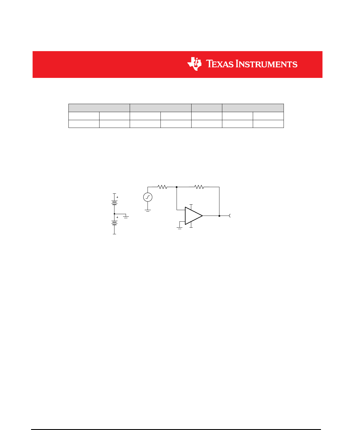
+
U1 LM7332
Vcc 15
Vee 15
+
Vi
Vo
4SBOA269A–February 2018–Revised January 2019
Submit Documentation Feedback
Copyright © 2018–2019, Texas Instruments Incorporated
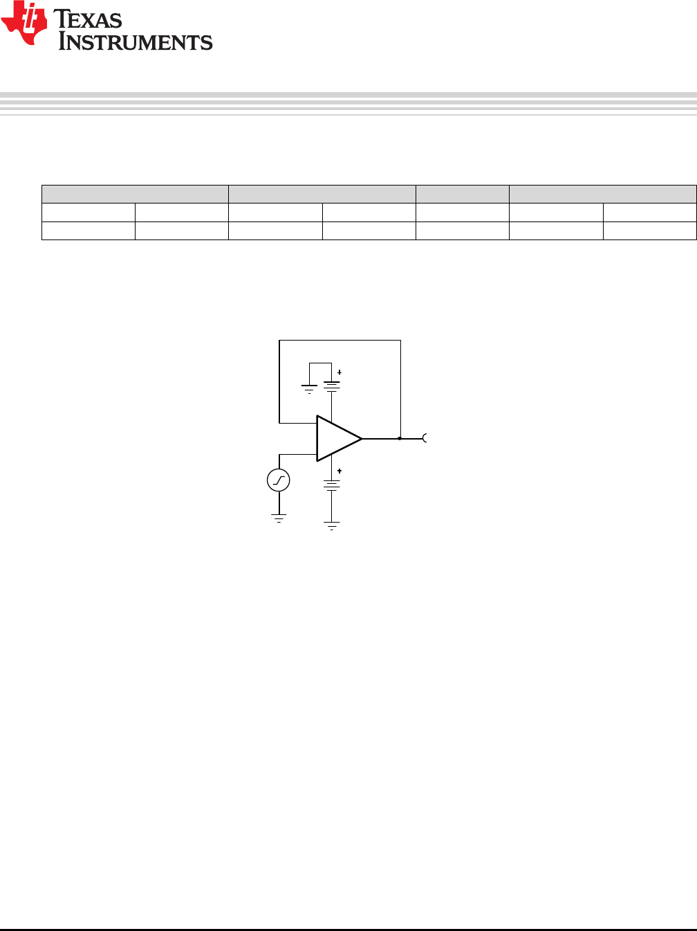
Buffer (follower) circuit
Analog Engineer's Circuit: Amplifiers
SBOA269A–February 2018–Revised January 2019
Buffer (follower) circuit
Design Goals
Input Output Freq. Supply
ViMin ViMax VoMin VoMax f Vcc Vee
–10V 10V –10V 10V 100kHz 15V –15V
Design Description
This design is used to buffer signals by presenting a high input impedance and a low output impedance.
This circuit is commonly used to drive low-impedance loads, analog-to-digital converters (ADC) and buffer
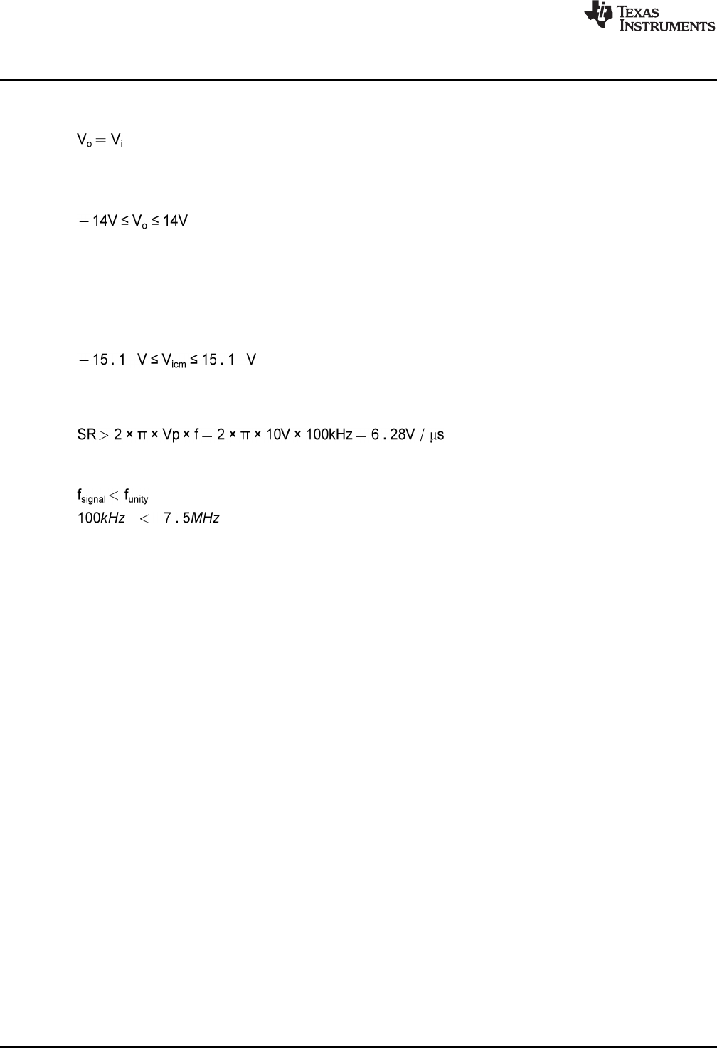
reference voltages. The output voltage of this circuit is equal to the input voltage.
Design Notes
1. Use the op-amp linear output operating range, which is usually specified under the AOL test conditions.
2. The small-signal bandwidth is determined by the unity-gain bandwidth of the amplifier.
3. Check the maximum output voltage swing versus frequency graph in the datasheet to minimize slew-
induced distortion.
4. The common mode voltage is equal to the input signal.
5. Do not place capacitive loads directly on the output that are greater than the values recommended in
the datasheet.
6. High output current amplifiers may be required if driving low impedance loads.
7. For more information on op-amp linear operating region, stability, slew-induced distortion, capacitive
load drive, driving ADCs, and bandwidth, see the Design References section.
www.ti.com
Design Steps
The transfer function for this circuit follows:
1. Verify that the amplifier can achieve the desired output swing using the supply voltages provided. Use
the output swing stated in the AOL test conditions. The output swing range of the amplifier must be
greater than the output swing required for the design.
• The output swing of the LM7332 using ±15-V supplies is greater than the required output swing of the
design. Therefore, this requirement is met.
• Review the Output Voltage versus Output Current curves in the product datasheet to verify the desired
output voltage can be achieved for the desired output current.
2. Verify the input common mode voltage of the amplifier will not be violated using the supply voltage
provided. The input common mode voltage range of the amplifier must be greater than the input signal
voltage range.
• The input common-mode range of the LM7332 using ±15-V supplies is greater than the required input
common-mode range of the design. Therefore, this requirement is met.
3. Calculate the minimum slew rate required to minimize slew-induced distortion.
• The slew rate of the LM7332 is 15.2V/µs. Therefore, this requirement is met.
4. Verify the device will have sufficient bandwidth for the desired output signal frequency.
• The desired output signal frequency is less than the unity-gain bandwidth of the LM7332. Therefore,
this requirement is met.
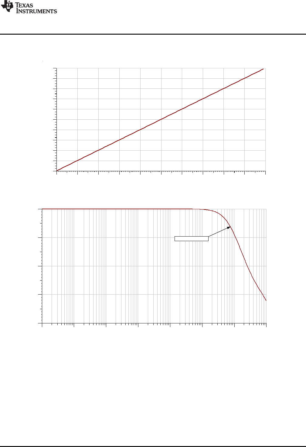
5SBOA269A–February 2018–Revised January 2019
Submit Documentation Feedback
Copyright © 2018–2019, Texas Instruments Incorporated
Buffer (follower) circuit
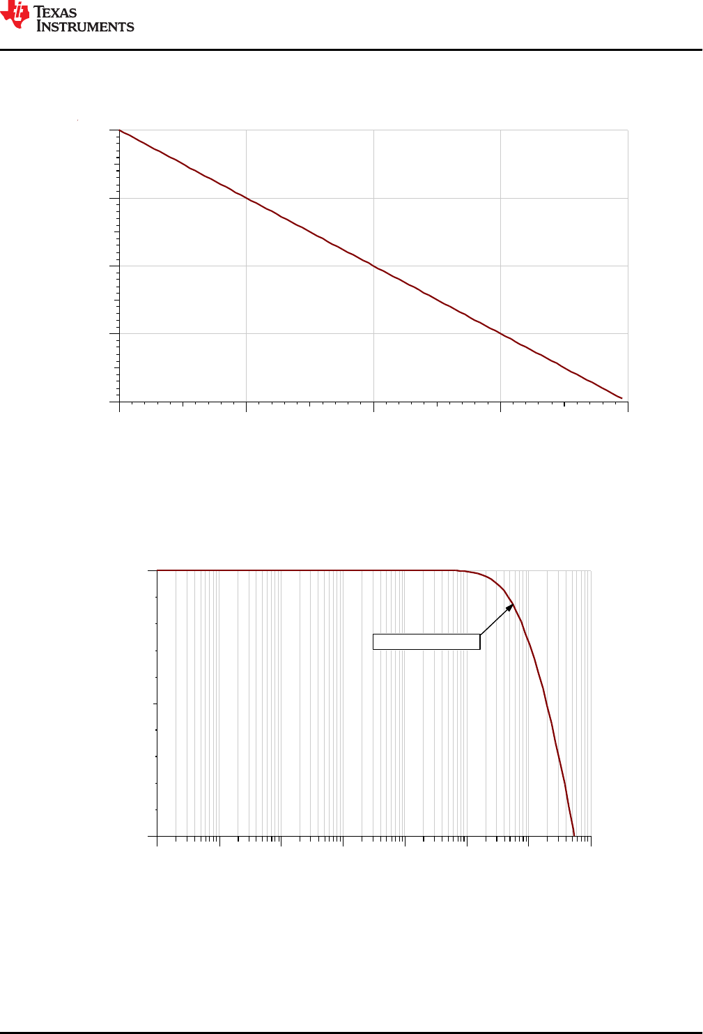
T
-3dB BW = 7.4MHz
Frequency (Hz)
10 100 1k 10k 100k 1MEG 10MEG 100MEG
G
ai
n
(d
B
)
-20
-15
-10
-5
0
-3dB BW = 7.4MHz
T
Input voltage (V)
-10 -8 -6 -4 -2 0 2 4 6 8 10
O
ut
pu
t V
ol
ta
ge
(V
)
-10
-8
-6
-4
-2
0
2
4
6
8
10
Input voltage (V)
-10 -8 -6 -4 -2 0 2 4 6 8 10
O
ut
pu
t V
ol
ta
ge
(V
)
-10
-8
-6
-4
-2
0
2
4
6
8
10
www.ti.com
6SBOA269A–February 2018–Revised January 2019
Submit Documentation Feedback
Copyright © 2018–2019, Texas Instruments Incorporated
Buffer (follower) circuit
Design Simulations
DC Simulation Results
AC Simulation Results
Design References
See the Analog Engineer's Circuit Cookbooksfor TI's comprehensive circuit library.
For more information, see the Capacitive Load Drive Verified Reference Design Using an Isolation
Resistor TI Design.
See the circuit SPICE simulation file SBOC491 – http://www.ti.com/lit/zip/sboc491.
For more information on many op amp topics including common-mode range, output swing, bandwidth,
slew rate, and how to drive an ADC, see TI Precision Labs.
www.ti.com
Design Featured Op Amp
LM7332
Vss 2.5V to 32V
VinCM Rail-to-rail
Vout Rail-to-rail
Vos 1.6mV
Iq 2mA
Ib 1µA
UGBW 7.5MHz (±5-V supply)
SR 15.2V/µs
#Channels 2
www.ti.com/product/LM7332
Design Alternate Op Amp
OPA192
Vss 4.5V to 36V
VinCM Rail-to-rail
Vout Rail-to-rail
Vos 5µV
Iq 1mA
Ib 5pA
UGBW 10MHz
SR 20V/µs
#Channels 1, 2, 4
www.ti.com/product/opa192
The following device is for battery-operated or power-conscious designs outside of the original design
goals described earlier, where lowering the total system power is desired.
LPV511
Vss 2.7V to 12V
VinCM Rail-to-rail
Vout Rail-to-rail
Vos 0.2mV
Iq 1.2µA
Ib 0.8nA
UGBW 27KHz
SR 7.5V/ms
#Channels 1
www.ti.com/product/lpv511
Revision History
Revision Date Change
A January 2019 Downscale title.
Added LPV511 table in the Design Alternate Op Amp section.
7SBOA269A–February 2018–Revised January 2019
Submit Documentation Feedback
Copyright © 2018–2019, Texas Instruments Incorporated
Buffer (follower) circuit
Analog Engineer’s Circuit Amplifiers
Inverting Amplifier Circuit
Design Goals
Input Output Freq. Supply
ViMin ViMax VoMin VoMax f Vcc Vee
–7V 7V –14V 14V 3kHz 15V –15V
Design Description
This design inverts the input signal, Vi, and applies a signal gain of –2V/V. The input signal typically comes from
a low-impedance source because the input impedance of this circuit is determined by the input resistor, R1. The
common-mode voltage of an inverting amplifier is equal to the voltage connected to the non-inverting node,
which is ground in this design.
Vcc
Vee
Vee
Vcc
Vo
R2 20kR1 10k
+
Vi
-
+
+
U1 TLV170
Vee 15
Vcc 15
Copyright © 2018, Texas Instruments Incorporated
Design Notes
1. Use the op amp in a linear operating region. Linear output swing is usually specified under the AOL test
conditions. The common-mode voltage in this circuit does not vary with input voltage.
2. The input impedance is determined by the input resistor. Make sure this value is large when compared to the
source output impedance.
3. Using high value resistors can degrade the phase margin of the circuit and introduce additional noise in the
circuit.
4. Avoid placing capacitive loads directly on the output of the amplifier to minimize stability issues.
5. Small-signal bandwidth is determined by the noise gain (or non-inverting gain) and op amp gain-bandwidth
product (GBP). Additional filtering can be accomplished by adding a capacitor in parallel to R2. Adding a
capacitor in parallel with R2 improves stability of the circuit if high value resistors are used.
6. Large signal performance can be limited by slew rate. Therefore, check the maximum output swing versus
frequency plot in the data sheet to minimize slew-induced distortion.
7. For more information on op amp linear operating region, stability, slew-induced distortion, capacitive load
drive, driving ADCs, and bandwidth, see the Design References section.
www.ti.com
SBOA270C – MARCH 2019 – REVISED DECEMBER 2020
Submit Document Feedback
Inverting Amplifier Circuit 8
Copyright © 2020 Texas Instruments Incorporated
Design Steps
The transfer function of this circuit follows:
Vo = Vi × ( -
R2
R1
)
1. Determine the starting value of R1. The relative size of R1 to the signal source impedance affects the gain
error. Assuming the impedance from the signal source is low (for example, 100Ω), set R1 = 10kΩ for 1% gain
error.
R1 = 10 kΩ
2. Calculate the gain required for the circuit. Since this is an inverting amplifier, use ViMin and VoMax for the
calculation.
G =
VoMax
ViMin
=
14 V
- 7 V
= - 2
V
V
3. Calculate R2 for a desired signal gain of –2 V/V.
G = -
R2
R1
→ R2 = - G × R1 = - ( - 2
V
V
) × 10 kΩ = 20 kΩ
4. Calculate the small signal circuit bandwidth to ensure it meets the 3-kHz requirement. Be sure to use the
noise gain, or non-inverting gain, of the circuit.
GBPTLV 170 = 1 . 2 MHz
NG = ( 1 +
R2
R1
) = 3
V
V
BW =
GBP
NG
=
1 . 2 MHz
3 V / V
= 400 kHz
5. Calculate the minimum slew rate required to minimize slew-induced distortion.
Vp =
SR
2 × π × f
→ SR > 2 × π × f × Vp
SR > 2 × π × 3 kHz × 14 V = 263 . 89
kV
s
= 0 . 26
V
μs
• SRTLV170 = 0.4V/µs, therefore, it meets this requirement.
6. To avoid stability issues, ensure that the zero created by the gain setting resistors and input capacitance of
the device is greater than the bandwidth of the circuit.
1
2 × π × ( Ccm + Cdiff ) × ( R2 ∥ R1 )
>
GBP
NG
1
2 × π × ( 3 pF + 3 pF ) ×
20 kΩ × 10 kΩ
20 kΩ + 10 kΩ
>
1 . 2 MHz
3 V / V
3.97 MHz 400 kHz!
• Ccm and Cdiff are the common-mode and differential input capacitance of the TLV170, respectively.
• Since the zero frequency is greater than the bandwidth of the circuit, this requirement is met.
www.ti.com
SBOA270C – MARCH 2019 – REVISED DECEMBER 2020
Submit Document Feedback
Inverting Amplifier Circuit 9
Copyright © 2020 Texas Instruments Incorporated
Design Simulations
DC Simulation Results
T
Input voltage (V)
-7.0 -3.5 0.0 3.5 7.0
V
o
lt
a
g
e
(
V
)
-14.0
-7.0
0.0
7.0
14.0
AC Simulation Results
The bandwidth of the circuit depends on the noise gain, which is 3V/V. The bandwidth is determined by looking
at the –3-dB point, which is located at 3dB given a signal gain of 6dB. The simulation sufficiently correlates with
the calculated value of 400kHz.
T
-3dB BW=519kHz
Frequency (Hz)
1 10 100 1k 10k 100k 1M 10M
G
a
in
(
d
B
)
-20.00
6.03
-3dB BW=519kHz
www.ti.com
SBOA270C – MARCH 2019 – REVISED DECEMBER 2020
Submit Document Feedback
Inverting Amplifier Circuit 10
Copyright © 2020 Texas Instruments Incorporated
Transient Simulation Results
The output is double the magnitude of the input and inverted.
T
Time (s)
0 250u 500u 750u 1m
V
o
lt
a
g
e
(
V
)
-13.99
0.00
13.99
www.ti.com
SBOA270C – MARCH 2019 – REVISED DECEMBER 2020
Submit Document Feedback
Inverting Amplifier Circuit 11
Copyright © 2020 Texas Instruments Incorporated
References:
1. Analog Engineer's Circuit Cookbooks
2. SPICE Simulation File SBOC492
3. TI Precision Labs
Design Featured Op Amp
TLV170
Vss ±18 V (36 V)
VinCM (Vee-0.1 V) to (Vcc-2 V)
Vout Rail-to-rail
Vos 0.5 mV
Iq 125 µA
Ib 10 pA
UGBW 1.2 MHz
SR 0.4 V/µs
#Channels 1, 2, 4
www.ti.com/product/tlv170
Design Alternate Op Amp
LMV358A
Vss 2.5 V to 5.5 V
VinCM (Vee–0.1 V) to (Vcc–1 V)
Vout Rail-to-rail
Vos 1 mV
Iq 70 µA
Ib 10 pA
UGBW 1 MHz
SR 1.7 V/µs
#Channels 1 (LMV321A), 2 (LMV358A), 4
(LMV324A)
www.ti.com/product/lmv358A
Revision History
Revision Date Change
C December 2020 Updated result for Design Step 6.
B March 2019 Changed LMV358 to LMV358A in the Design Alternate Op Amp section.
A January 2019 Downstyle title.
Added link to circuit cookbook landing page.
www.ti.com
SBOA270C – MARCH 2019 – REVISED DECEMBER 2020
Submit Document Feedback
Inverting Amplifier Circuit 12
Copyright © 2020 Texas Instruments Incorporated
VEE 15
VCC 15
-
+
+
U1 OPA171
+
Vi
R1 9.09k
Vo
R2 1.01k
13SBOA271A–January 2018–Revised January 2019
Submit Documentation Feedback
Copyright © 2018–2019, Texas Instruments Incorporated
Non-inverting amplifier circuit
Analog Engineer's Circuit: Amplifiers
SBOA271A–January 2018–Revised January 2019
Non-inverting amplifier circuit
Design Goals
Input Output Supply
ViMin ViMax VoMin VoMax Vcc Vee
–1V 1V –10V 10 15V –15V
Design Description
This design amplifies the input signal, Vi, with a signal gain of 10V/V. The input signal may come from a
high-impedance source (for example, MΩ) because the input impedance of this circuit is determined by
the extremely high input impedance of the op amp (forexample, GΩ). The common-mode voltage of a
non-inverting amplifier is equal to the input signal.
Design Notes
1. Use the op amp linear output operating range, which is usually specified under the AOL test conditions.
The common-mode voltage is equal to the input signal.
2. The input impedance of this circuit is equal to the input impedance of the amplifier.
3. Using high-value resistors can degrade the phase margin of the circuit and introduce additional noise
in the circuit.
4. Avoid placing capacitive loads directly on the output of the amplifier to minimize stability issues.
5. The small-signal bandwidth of a non-inverting amplifier depends on the gain of the circuit and the gain
bandwidth product (GBP) of the amplifier. Additional filtering can be accomplished by adding a
capacitor in parallel to R1. Adding a capacitor in parallel with R1 will also improve stability of the circuit
if high-value resistors are used.
6. Large signal performance may be limited by slew rate. Therefore, check the maximum output swing
versus frequency plot in the data sheet to minimize slew-induced distortion.
7. For more information on op amp linear operating region, stability, slew-induced distortion, capacitive
load drive, driving ADCs, and bandwidth please see the Design References section.
www.ti.com
Design Steps
The transfer function for this circuit is given below.
1. Calculate the gain.
2. Calculate values for R1 and R2.
3. Calculate the minimum slew rate required to minimize slew-induced distortion.
• The slew rate of the OPA171 is 1.5V/µs, therefore it meets this requirement.
4. To maintain sufficient phase margin, ensure that the zero created by the gain setting resistors and
input capacitance of the device is greater than the bandwidth of the circuit.
• Ccm and Cdiff are the common-mode and differential input capacitances of the OPA171, respectively.
• Since the zero frequency is greater than the bandwidth of the circuit, this requirement is met.
14SBOA271A–January 2018–Revised January 2019
Submit Documentation Feedback
Copyright © 2018–2019, Texas Instruments Incorporated
Non-inverting amplifier circuit
T
-3dB BW = 323.2kHz
Frequency (Hz)
10 100 1k 10k 100k 1MEG 10MEG 100MEG
G
ai
n
(d
B
)
-40
-30
-20
-10
0
10
20
-3dB BW = 323.2kHz
T
Input voltage (V)
-1 -750m -500m -250m 0 250m 500m 750m 1
O
ut
pu
t V
ol
ta
ge
(V
)
-10
-8
-6
-4
-2
0
2
4
6
8
10
www.ti.com
15SBOA271A–January 2018–Revised January 2019
Submit Documentation Feedback
Copyright © 2018–2019, Texas Instruments Incorporated
Non-inverting amplifier circuit
Design Simulations
DC Simulation Results
AC Simulation Results
www.ti.com
Design References
See Analog Engineer's Circuit Cookbooks for TI's comprehensive circuit library.
See circuit SPICE simulation file SBOC493.
For more information on many op amp topics including common-mode range, output swing, and
bandwidth please visit TI Precision Labs.
Design Featured Op Amp
OPA171
Vss 2.7V to 36V
VinCM (Vee–0.1V) to (Vcc–2V)
Vout Rail-to-rail
Vos 250µV
Iq 475µA
Ib 8pA
UGBW 3MHz
SR 1.5V/µs
#Channels 1, 2, 4
www.ti.com/product/opa171
Design Alternate Op Amp
OPA191
Vss 4.5V to 36V
VinCM Rail-to-rail
Vout Rail-to-rail
Vos 5µV
Iq 140µA
Ib 5pA
UGBW 2.5MHz
SR 7.5V/µs
#Channels 1, 2, 4
www.ti.com/product/OPA191
Revision History
Revision Date Change
A January 2019 Downscale the title and changed title role to 'Amplifiers'.
Added link to circuit cookbook landing page.
16SBOA271A–January 2018–Revised January 2019
Submit Documentation Feedback
Copyright © 2018–2019, Texas Instruments Incorporated
Non-inverting amplifier circuit
Analog Engineer’s Circuit Amplifiers
Inverting Summer Circuit
Design Goals
Input 1 Input 2 Output Freq. Supply
Vi1Min Vi1Max Vi2Min Vi2Max VoMin VoMax f Vcc Vee
–2.5V 2.5V –250mV 250mV –4.9V 4.9V 10kHz 5V –5V
Design Description
This design sums (adds) and inverts two input signals, Vi1 and Vi2. The input signals typically come from low-
impedance sources because the input impedance of this circuit is determined by the input resistors, R1 and R2.
The common-mode voltage of an inverting amplifier is equal to the voltage connected to the non-inverting node,
which is ground in this design.
VCC
VCC
VEE
VEE
R2 2.05 k
R1 20.5 k
R3 20 k
VCC 5
+
Vi1
VO
VEE 5
-
+
+
U1 TLV170
+
Vi2
+
+
Design Notes
1. Use the op amp in a linear operating region. Linear output swing is usually specified under the AOL test
conditions. The common-mode voltage in this circuit does not vary with input voltage.
2. The input impedance is determined by the input resistors. Make sure these values are large when compared
to the output impedance of the source.
3. Using high-value resistors can degrade the phase margin of the circuit and introduce additional noise in the
circuit.
4. Avoid placing capacitive loads directly on the output of the amplifier to minimize stability issues.
5. Small-signal bandwidth is determined by the noise gain (or non-inverting gain) and op amp gain-bandwidth
product (GBP). Additional filtering can be accomplished by adding a capacitor in parallel to R3. Adding a
capacitor in parallel with R3 will also improve stability of the circuit if high-value resistors are used.
6. Large signal performance may be limited by slew rate. Therefore, check the maximum output swing versus
frequency plot in the data sheet to minimize slew-induced distortion.
7. For more information on op amp linear operating region, stability, slew-induced distortion, capacitive load
drive, driving ADCs, and bandwidth please see the Design References section.
www.ti.com
SBOA272C – DECEMBER 2020 – REVISED JANUARY 2021
Submit Document Feedback
Inverting Summer Circuit 17
Copyright © 2021 Texas Instruments Incorporated
Design Steps
The transfer function for this circuit is given below.
8K = 8E1× lF
43
41
p+ 8E2× lF
43
42
p
1. Select a reasonable resistance value for R3.
43 = 20 GÀ
2. Calculate gain required for Vi1. For this design, half of the output swing is devoted to each input.
�)8E1� = n 8K/=T F8K/EJ2
8E1/=T F8E1/EJ
n= n4.9 8F :F4.9 8;2
2.5 8F :F2.5 8;n = 0.9888 = F0.175 @$
3. Calculate the value of R1.
�)8E1�=
43
41
\ 41 =
43
�)8E1�
=
20 GÀ
0.98
8
8
= 20.4 GÀN 20.5 GÀ (5P=J@=N@ 8=HQA)
4. Calculate gain required for Vi2. For this design, half of the output swing is devoted to each input.
�)8E2� = n 8K/=T F8K/EJ2
8E2/=T F8E2/EJ
n = n 4.9 8F (F4.9 8)2
250 I8F (F250 I8)
n= 9.8 8
8
= 19.82 @$
5. Calculate the value of R2.
�)8E2�=
43
42
\ 42 =
43
�)8E 2�
=
20 GÀ
9.8
8
8
= 2.04 GÀN 2.05 GÀ (5P=J@=N@ 8=HQA)
6. Calculate the small signal circuit bandwidth to ensure it meets the 10-kHz requirement. Be sure to use the
noise gain (NG), or non-inverting gain, of the circuit. When calculating the noise gain note that R1 and R2 are
in parallel.
)$212#170 = 1.2 /*V
0) = 1 +
43
41 ||42
= 1 +
20 GÀ
1.86 GÀ
= 11.75
8
8
= 21.4 @$
(8)
$9 =
)$2
0)
=
1.2 /*V
11.75
8
8
= 102 G*V
(9)
• This requirement is met because the closed-loop bandwidth is 102kHz and the design goal is 10kHz.
7. Calculate the minimum slew rate to minimize slew-induced distortion.
8L =
54
2 ×è × B
\ 54 > 2 × è× B × 8L
54 > 2 × è × 10 G*V× 4.9 8= 307.87
G8
O
= 0.31
8
µO (11)
• SROPA170=0.4V/µs, therefore it meets this requirement.
8. To avoid stability issues ensure that the zero created by the gain setting resistors and input capacitance of
the device is greater than the bandwidth of the circuit.
1
2 × è× k%?I +%@EBB o× :41 |�42�|43;
>
)$2
0)
1
2 × è × 3 L( × 3 L(× 1.7 GÀ
>
1.2 /*V
11.75
8
8 (13)
15.6 /*V> 102 G*V (14)
• Ccm and Cdiff are the common-mode and differential input capacitances.
• Since the zero frequency is greater than the bandwidth of the circuit, this requirement is met.
www.ti.com
Copyright © 2021 Texas Instruments Incorporated
SBOA272C – DECEMBER 2020 – REVISED JANUARY 2021
Submit Document Feedback
Inverting Summer Circuit 18
Design Simulations
DC Simulation ResultsThis simulation sweeps Vi1 from –2.5V to 2.5V while Vi2 is held constant at 0V. The output is inverted and ranges
from –2.44V to 2.44V.
T
Vo=2.44V
Vo=-2.44V
Input voltage (Vi1)
-2.5 0.0 2.5
V
o
lt
a
g
e
(
V
)
-2.5
0.0
2.5
Vo=-2.44V
Vo=2.44V
Vi2 held constant (0V)
Vi1 swept from -2.5V to 2.5V
This simulation sweeps Vi2 from –250mV to 250mV while Vi1 is held constant at 0V. The output is inverted and
ranges from –2.44V to 2.44V.
T
Vo=2.44V
Vo=-2.44V
Input voltage (Vi2)
-250.00m 0.00 250.00m
V
o
lt
a
g
e
(
V
)
-2.5
0.0
2.5
Vo=-2.44V
Vo=2.44V
Vi1 held constant (0V)
Vi2 swept from -250mV to 250mV
www.ti.com
SBOA272C – DECEMBER 2020 – REVISED JANUARY 2021
Submit Document Feedback
Inverting Summer Circuit 19
Copyright © 2021 Texas Instruments Incorporated
AC Simulation Results
This simulation shows the bandwidth of the circuit. Note that the bandwidth is the same for either input. This is
because the bandwidth depends on the noise gain of the circuit, not the signal gain of each input. These results
correlate well with the calculations.
T
Vi1
G=-0.21dB=0.98V/V
BW=114.86kHz
Vi2
G=19.79dB=9.76V/V
BW=114.7kHz
Frequency (Hz)
10 100 1k 10k 100k 1M 10M
G
a
in
(
d
B
)
-40
-20
0
20
BW=114.86kHz
BW=114.7kHz
Vi2
G=19.79dB=9.76V/V
Vi1
G=-0.21dB=0.98V/V
Transient Simulation Results
This simulation shows the inversion and summing of the two input signals. Vi1 is a 1-kHz, 5-Vpp sine wave and
Vi2 is a 10-kHz, 500-mVpp sine wave. Since both inputs are properly amplified or attenuated, the output is within
specification.
T
Time (s)
0.00 1.50m 3.00m
Vi1
-2.50
2.50
Vi2
-250.00m
250.00m
Vo
-4.84
4.85
www.ti.com
Copyright © 2021 Texas Instruments Incorporated
SBOA272C – DECEMBER 2020 – REVISED JANUARY 2021
Submit Document Feedback
Inverting Summer Circuit 20
Design References
See Analog Engineer's Circuit Cookbooks for TI's comprehensive circuit library.
See circuit SPICE simulation file SBOC494.
For more information on many op amp topics including common-mode range, output swing, bandwidth, and how
to drive an ADC please visit TI Precision Labs.
Design Featured Op Amp
OPA170
Vss 2.7V to 36V
VinCM (Vee-0.1V) to (Vcc-2V)
Vout Rail-to-rail
Vos 0.25mV
Iq 110µA
Ib 8pA
UGBW 1.2MHz
SR 0.4V/µs
#Channels 1, 2, 4
www.ti.com/product/opa170
Design Alternate Op Amp
LMC7101
Vss 2.7V to 15.5V
VinCM Rail-to-rail
Vout Rail-to-rail
Vos 110µV
Iq 0.8mA
Ib 1pA
UGBW 1.1MHz
SR 1.1V/µs
#Channels 1
www.ti.com/product/lmc7101
Revision History
Revision Date Change
C January 2021 Updated Formula format
B December 2020 Updated Design Goals Table
A January 2019 Down-style title.
Updated title role to Amplifiers.
Added link to circuit cookbook landing page.
www.ti.com
SBOA272C – DECEMBER 2020 – REVISED JANUARY 2021
Submit Document Feedback
Inverting Summer Circuit 21
Copyright © 2021 Texas Instruments Incorporated
Vcc
Vee
Vcc
Vref
Vee
Vref
Vo
R3 20kR1 10k
-
+
+
U1 TLV6001
R2 10k
Vcc 2.75
R4 20k
Vee 2.75
Vref 0
Vi1
Vi2
+
+
+
+
+
Copyright © 2018, Texas Instruments Incorporated
22SBOA274A–February 2018–Revised January 2019
Submit Documentation Feedback
Copyright © 2018–2019, Texas Instruments Incorporated
Difference amplifier (subtractor) circuit
Analog Engineer's Circuit: Amplifiers
SBOA274A–February 2018–Revised January 2019
Difference amplifier (subtractor) circuit
Design Goals
Input (Vi2-Vi1) Output CMRR (min) Supply
VidiffMin VidiffMax VoMin VoMax dB Vcc Vee Vref
–1.25V 1.25V –2.5V 2.5V 50 2.75V –2.75V 0V
Design Description
This design inputs two signals, Vi1 and Vi2, and outputs their difference (subtracts). The input signals
typically come from low-impedance sources because the input impedance of this circuit is determined by
the resistive network. Difference amplifiers are typically used to amplify differential input signals and reject
common-mode voltages. A common-mode voltage is the voltage common to both inputs. The
effectiveness of the ability of a difference amplifier to reject a common-mode signal is known as common-
mode rejection ratio (CMRR). The CMRR of a difference amplifier is dominated by the tolerance of the
resistors.
Design Notes
1. Use the op amp in a linear operating region. Ensure that the inputs of the op amp do not exceed the
common-mode range of the device. Linear output swing is usually specified under the AOL test
conditions.
2. The input impedance is determined by the input resistive network. Make sure these values are large
when compared to the output impedance of the sources.
3. Using high-value resistors can degrade the phase margin of the circuit and introduce additional noise
in the circuit.
4. Avoid placing capacitive loads directly on the output of the amplifier to minimize stability issues.
5. Small-signal bandwidth is determined by the noise gain (or non-inverting gain) and op amp gain-
bandwidth product (GBP). Additional filtering can be accomplished by adding a capacitors in parallel to
R3 and R4. Adding capacitors in parallel with R3 and R4 will also improve stability of the circuit if high-
value resistors are used.
6. Large signal performance may be limited by slew rate. Therefore, check the maximum output swing
versus frequency plot in the data sheet to minimize slew-induced distortion.
7. For more information on op amp linear operating region, stability, slew-induced distortion, capacitive
load drive, driving ADCs, and bandwidth please see the Design References section.
www.ti.com
Copyright © 2018–2019, Texas Instruments Incorporated
Design Steps
The complete transfer function for this circuit is shown below.
If R1 = R2 and R3 = R4 the transfer function for this circuit simplifies to the following equation.
• Where the gain, G, is R3/R1.
1. Determine the starting value of R1 and R2. The relative size of R1 and R2 to the signal impedance of the
source affects the gain error.
2. Calculate the gain required for the circuit.
3. Calculate the values for R3 and R4.
4. Calculate resistor tolerance to meet the minimum common-mode rejection ratio (CMRR). For minimum
(worst-case) CMRR, α = 4. For a more probable, or typical value of CMRR, α = 0.33.
5. For quick reference, the following table compares resistor tolerance to minimum and typical CMRR
values assuming G = 1 or G = 2. As shown above, as gain increases so does CMRR.
Tolerance G=1 Minimum (dB) G=1 Typical (dB) G=2 Minimum (dB) G=2 Typical (dB)
0.01%=0.0001 74 95.6 77.5 99.2
0.1%=0.001 54 75.6 57.5 79.2
0.5%=0.005 40 61.6 43.5 65.2
1%=0.01 34 55.6 37.5 59.2
5%=0.05 20 41.6 23.5 45.2
23SBOA274A–February 2018–Revised January 2019
Submit Documentation Feedback
Difference amplifier (subtractor) circuit
T
Worst Case CMRR=-51.11dB
Data sheets typically depict CMRR as
a positive number.
Frequency (Hz)
10 20
G
ai
n
(d
B
)
-80
-60
-40
Worst Case CMRR=-51.11dB
Data sheets typically depict CMRR as
a positive number.
This value is referred to the output.
To refer to input, subtract the gain in dB,
which is 6dB (2V/V). Actual CMRR
referred to the input is therefore -57.11dB
T
Input voltage (Vdiff)
-1.25 -750.00m -250.00m 250.00m 750.00m 1.25
O
ut
pu
t
-2.5
-1.5
-500.0m
500.0m
1.5
2.5
Vdiff=Vi2-Vi1
www.ti.com
24SBOA274A–February 2018–Revised January 2019
Submit Documentation Feedback
Copyright © 2018–2019, Texas Instruments Incorporated
Difference amplifier (subtractor) circuit
Design Simulations
DC Simulation Results
CMRR Simulation Results
www.ti.com
Copyright © 2018–2019, Texas Instruments Incorporated
Design References
See Analog Engineer's Circuit Cookbooks for TI's comprehensive circuit library.
See circuit SPICE simulation file SBOC495.
For more information on many op amp topics including common-mode range, output swing, bandwidth,
and how to drive an ADC please visit TI Precision Labs. For more information on difference amplifier
CMRR, please read Overlooking the obvious: the input impedance of a difference amplifier .
Design Featured Op Amp
TLV6001
Vss 1.8V to5.5V
VinCM Rail-to-rail
Vout Rail-to-rail
Vos 750µV
Iq 75µA
Ib 1pA
UGBW 1MHz
SR 0.5V/µs
#Channels 1, 2, 4
www.ti.com/product/tlv6001
Design Alternate Op Amp
OPA320
Vss 1.8V to 5.5V
VinCM Rail-to-rail
Vout Rail-to-rail
Vos 40µV
Iq 1.5mA
Ib 0.2pA
UGBW 20MHz
SR 10V/µs
#Channels 1, 2
www.ti.com/product/opa320
Revision History
Revision Date Change
A January 2019 Downscale title.
Added link to circuit cookbook landing page.
25SBOA274A–February 2018–Revised January 2019
Submit Documentation Feedback
Difference amplifier (subtractor) circuit
V-
V+
V-
V+
Vref
Vref
V-
V+
R1 5.1k
R3 5.1k R2 20k
R4 20k
Vo
Rg 7.87k
Vcm
C
1
1
00
n
C
2
1
00
n
Vcc 15
Vee 15
-
U2 TLV171
Vref 0
-
U1 TLV171
+
Vi2
+
Vi1
+
+
+
+
26SBOA281–December 2018
Submit Documentation Feedback
Copyright © 2018, Texas Instruments Incorporated
Two op amp instrumentation amplifier circuit
Analog Engineer's Circuit: Amplifiers
SBOA281–December 2018
Two op amp instrumentation amplifier circuit
Design Goals
Input ViDiff(Vi2 - Vi1) Output Supply
ViDiff_Min ViDiff_Max VoMin VoMax Vcc Vee Vref
+/–1V +/–2V –10V +10V 15V –15V 0V
Vcm Gain Range
+/-10V 5V/V to 10V/V
Design Description
This design amplifiers the difference between Vi1 and Vi2 and outputs a single ended signal while rejecting
the common–mode voltage. Linear operation of an instrumentation amplifier depends upon the linear
operation of its primary building block: op amps. An op amp operates linearly when the input and output
signals are within the device’s input common–mode and output–swing ranges, respectively. The supply
voltages used to power the op amps define these ranges.
Design Notes
1. Rg sets the gain of the circuit.
2. High–value resistors can degrade the phase margin of the circuit and introduce additional noise in the
circuit.
3. The ratio of R4 and R3 set the minimum gain when Rg is removed.
4. Ratios of R2/R1 and R4/R3 must be matched to avoid degrading the instrumentation amplifier’s DC
CMRR and ensuring the Vref gain is 1V/V.
5. Linear operation is contingent upon the input common–mode and the output swing ranges of the
discrete op amps used. The linear output swing ranges are specified under the Aol test conditions in
the op amps datasheets.
www.ti.com
Design Steps
1. Transfer function of this circuit.
2. Select R4 and R3 to set the minimum gain.
3. Select R1 and R2. Ensure that R1/R2 and R3/R4 ratios are matched to set the gain applied to the
reference voltage at 1V/V.
4. Select Rg to meet the desired maximum gain G = 10V/V.
27SBOA281–December 2018
Submit Documentation Feedback
Two op amp instrumentation amplifier circuit
Copyright © 2018, Texas Instruments Incorporated
T
Time (s)
0.00 2.50m 5.00m
Vi1
-499.56m
499.70m
Vi2
-499.70m
499.56m
Vi2 - Vi1
-1.00
1.00
Vo
-10.00
10.00
T
Time (s)
0.00 2.50m 5.00m
Vi1
-997.45m
997.45m
Vi2
-997.45m
997.45m
Vi2 - Vi1
-2.00
2.00
Vo
-9.82
9.82
T
Vo=9.8V when Vdiff=1
regardless of the
common-mode voltage
Common-Mode voltage (Vcm)
-10.00 0.00 10.00
V
ol
ta
ge
(
V
o)
9.00
10.00
11.00
Vo=9.8V when Vdiff=1
regardless of the
common-mode voltage
www.ti.com
28SBOA281–December 2018
Submit Documentation Feedback
Copyright © 2018, Texas Instruments Incorporated
Two op amp instrumentation amplifier circuit
Design Simulations
DC Simulation Results
Transient Simulation Results
www.ti.com
References:
1. Analog Engineer's Circuit Cookbooks
2. SPICE Simulation File SBOMAU7
3. TI Precision Labs
4. VCM vs. VOUT plots for instrumentation amplifiers with two op amps
5. Common-mode Range Calculator for Instrumentation Amplifiers
Design Featured Op Amp
TLV171
Vss 4.5V to 36V
VinCM (Vee–0.1V) to (Vcc–2V)
Vout Rail–to–rail
Vos 0.25mV
Iq 475µA
Ib 8pA
UGBW 3MHz
SR 1.5V/µs
#Channels 1,2,4
www.ti.com/product/tlv171
Design Alternate Op Amp
OPA172
Vss 4.5V to 36V
VinCM (Vee–0.1V) to (Vcc–2V)
Vout Rail–to–rail
Vos 0.2mV
Iq 1.6mA
Ib 8pA
UGBW 10MHz
SR 10V/µs
#Channels 1,2,4
www.ti.com/product/opa172
29SBOA281–December 2018
Submit Documentation Feedback
Two op amp instrumentation amplifier circuit
Copyright © 2018, Texas Instruments Incorporated
Analog Engineer's Circuit
Three Op Amp Instrumentation Amplifier Circuit
Amplifiers
Design Goals
Input Vidiff (Vi2 – Vi1)
Common-
Mode Voltage Output Supply
Vi diff Min Vi diff Max Vcm VoMin VoMax Vcc Vee Vref
-0.5 V +0.5 V ±7 V –5 V +5 V +15 V –15 V 0 V
Design Description
This design uses 3 op amps to build a discrete instrumentation amplifier. The circuit converts a differential signal
to a single-ended output signal. Linear operation of an instrumentation amplifier depends upon linear operation
of its building block: op amps. An op amp operates linearly when the input and output signals are within the
device’s input common-mode and output swing ranges, respectively. The supply voltages used to power the op
amps define these ranges.
V-
V+
V-
V+
V-
V+
Vref
V-
V+
Vref
-
+
+
U1 TLV171
-
+
+
U2 TLV171
R5 10k
-
+
+
U3 TLV171
R6 10k
R3 10k
R1 10k
R2 10k
Vo
R4 10k
R10
2.21k
+
Vi2
+
Vi1
C
1
1
0
0
n
C
2
1
0
0
n
Vcc 15
Vee 15
Vref 0
Vcm
Design Notes
1. Use precision resistors to achieve high DC CMRR performance
2. R10 sets the gain of the circuit.
3. Add an isolation resistor to the output stage to drive large capacitive loads.
4. High-value resistors can degrade the phase margin of the circuit and introduce additional noise in the circuit.
5. Linear operation is contingent upon the input common-mode and the output swing ranges of the discrete op
amps used. The linear output swing ranges are specified under the Aol test conditions in the op amps data
sheets.
www.ti.com
SBOA282A – DECEMBER 2018 – REVISED MARCH 2022
Submit Document Feedback
Three Op Amp Instrumentation Amplifier Circuit 30
Copyright © 2022 Texas Instruments Incorporated
Design Steps
1. Transfer function of this circuit:
( )= - ´ +O i2 i1 refV V V G V
When Vref = 0, the transfer function simplifies to the following equation:
( )= - ´O i2 i1V V V G
where
æ ö´
= ´ +ç ÷
è ø
54
3 10
2 RR
G 1
R R
2. Select the feedback loop resistors R5 and R6:
= = W5 6Choose R R 10 k (Standard Value)
3. Select R1, R2, R3, R4. To set the Vref gain at 1 V/V and avoid degrading the instrumentation amplifier's
CMRR, ratios of R4/R3 and R2/R1 must be equal.
= = = = W1 2 3 4Choose R R R R 10 k (Standard Value)
4. Calculate R10 to meet the desired gain:
æ ö´
= ´ + =ç ÷
è ø
54
3 10
2 RR VG 1 10
R R V
= = W4 3R R 10 k
æ ö æ ö´ W W
® = + = ® + =ç ÷ ç ÷
è ø è ø10 10
2 10k V 20k VG 1 10 1 10
R V R V
( )
W W
= ® = = W ® = W10 10
10
20 k V 20 k9 R 2222.2 R 2.21k Standard Value
R V 9
5. To check the common-mode voltage range, download and install the program from reference [5]. Edit the
INA_Data.txt file in the installation directory by adding the code for a 3 op amp INA whose internal amplifiers
have the common-mode range, output swing, and supply voltage range as defined by the amplifier of choice
(TLV172, in this case). There is no Vbe shift in this design and the gain of the output stage difference
amplifeir is 1 V/V. The default supply voltage and reference voltages are ±15 V and 0 V, respectively.
Run the program and set the gain and reference voltage accordingly. The resulting VCM vs. VOUT plot
approximates the linear operating region of the discrete INA.
www.ti.com
Copyright © 2022 Texas Instruments Incorporated
SBOA282A – DECEMBER 2018 – REVISED MARCH 2022
Submit Document Feedback
Three Op Amp Instrumentation Amplifier Circuit 31
Design Simulations
DC Simulation Results
T
Vo = 10.05V regardless of Vcm
Input voltage (V)
-2.00 -1.00 0.00 1.00 2.00
V
o
lt
a
g
e
(
V
)
9.00
10.00
11.00
Vo = 10.05V regardless of Vcm
Transient Simulation Results
T
Time (s)
0.00 1.00m 2.00m 3.00m 4.00m 5.00m 6.00m 7.00m
Vi1
-249.46m
249.46m
Vi2
-249.46m
249.46m
Vi2 - Vi1
-500.00m
500.00m
Vo
-5.01
5.02
www.ti.com
SBOA282A – DECEMBER 2018 – REVISED MARCH 2022
SubmitDocument Feedback
Three Op Amp Instrumentation Amplifier Circuit 32
Copyright © 2022 Texas Instruments Incorporated
References:
1. Analog Engineer's Circuit Cookbooks
2. SPICE Simulation File SBOMAU8
3. TI Precision Labs
4. Instrumentation Amplifier VCM vs. VOUT Plots
5. Common-mode Range Calculator for Instrumentation Amplifiers
Design Featured Op Amp
TLV171
Vss 4.5 V to 36 V
VinCM (V–) – 0.1 V < Vin < (V+) – 2 V
Vout Rail–to–rail
Vos 0.25 mV
Iq 475 µA
Ib 8 pA
UGBW 3 MHz
SR 1.5 V/µs
#Channels 1,2, and4
TLV171
Design Alternate Op Amp
OPA172 OPA192
Vss 4.5 V to 36 V 4.5 V to 36 V
VinCM
(V–) – 0.1 V < Vin <
(V+) – 2 V
Vee–0.1 V to Vcc+0.1
V
Vout Rail–to–rail Rail–to–rail
Vos 0.2 mV ±5 µV
Iq 1.6 mA 1 mA/Ch
Ib 8 pA 5 pA
UGBW 10 MHz 10 MHz
SR 10 V/µs 20 V/µs
#Channels 1, 2, and 4 1, 2, and 4
OPA172 OPA192
www.ti.com
Copyright © 2022 Texas Instruments Incorporated
SBOA282A – DECEMBER 2018 – REVISED MARCH 2022
Submit Document Feedback
Three Op Amp Instrumentation Amplifier Circuit 33
Vcc
Vee
Vee
Vcc
R1 100k C1 1.59n
+
Vin
Vout
R2 100M
Vos -740u
-
+
+
U1 TLV9002
Vcc 2.5
Vee 2.5
Copyright © 2018, Texas Instruments Incorporated
34SBOA275A–February 2018–Revised January 2019
Submit Documentation Feedback
Copyright © 2018–2019, Texas Instruments Incorporated
Integrator circuit
Analog Engineer's Circuit: Amplifiers
SBOA275A–February 2018–Revised January 2019
Integrator circuit
Design Goals
Input Output Supply
fMin f0dB fMax VoMin VoMax Vcc Vee
100Hz 1kHz 100kHz –2.45V 2.45V 2.5V –2.5V
Design Description
The integrator circuit outputs the integral of the input signal over a frequency range based on the circuit
time constant and the bandwidth of the amplifier. The input signal is applied to the inverting input so the
output is inverted relative to the polarity of the input signal. The ideal integrator circuit will saturate to the
supply rails depending on the polarity of the input offset voltage and requires the addition of a feedback
resistor, R2, to provide a stable DC operating point. The feedback resistor limits the lower frequency range
over which the integration function is performed. This circuit is most commonly used as part of a larger
feedback/servo loop which provides the DC feedback path, thus removing the requirement for a feedback
resistor.
Design Notes
1. Use as large of a value as practical for the feedback resistor.
2. Select a CMOS op amp to minimize the errors from the input bias current.
3. The gain bandwidth product (GBP) of the amplifier will set the upper frequency range of the integrator
function. The effectiveness of the integration function is usually reduced starting about one decade
away from the amplifier bandwidth.
4. An adjustable reference needs to be connected to the non-inverting input of the op amp to cancel the
input offset voltage or the large DC noise gain will cause the circuit to saturate. Op amps with very low
offset voltage may not require this.
T
-38.6dB @ 100kHz
40dB @ 10Hz
0dB @ 1kHz
Frequency (Hz)
1 10 100 1k 10k 100k 1M
G
ai
n
(d
B
)
-60
-40
-20
0
20
40
60
0dB @ 1kHz
40dB @ 10Hz
-38.6dB @ 100kHz
www.ti.com
Copyright © 2018–2019, Texas Instruments Incorporated
Design Steps
The ideal circuit transfer function is given below.
1. Set R1 to a standard value.
2. Calculate C1 to set the unity-gain integration frequency.
3. Calculate R2 to set the lower cutoff frequency a decade less than the minimum operating frequency.
4. Select an amplifier with a gain bandwidth at least 10 times the desired maximum operating frequency.
Design Simulations
AC Simulation Results
35SBOA275A–February 2018–Revised January 2019
Submit Documentation Feedback
Integrator circuit
Time (s)
100m 102.5m 105m
Vin
-100m
100m
Vout
-76.77m
77.53m
Time (s)
100m 102.5m 105m
Vin
-100m
0
100m
Vout
-100m
0
100m
www.ti.com
36SBOA275A–February 2018–Revised January 2019
Submit Documentation Feedback
Copyright © 2018–2019, Texas Instruments Incorporated
Integrator circuit
Transient Simulation Results
A 1-kHz sine wave input yields a 1-kHz cosine output.
A 1-kHz triangle wave input yields a 1-kHz sine wave output.
T
Time (s)
100m 102.5m 105m
Vin
-100m
100m
Vout
-136.45m
186.58m
www.ti.com
Copyright © 2018–2019, Texas Instruments Incorporated
A 1-kHz square wave input yields a 1-kHz triangle wave output.
37SBOA275A–February 2018–Revised January 2019
Submit Documentation Feedback
Integrator circuit
www.ti.com
38SBOA275A–February 2018–Revised January 2019
Submit Documentation Feedback
Copyright © 2018–2019, Texas Instruments Incorporated
Integrator circuit
Design References
See Analog Engineer's Circuit Cookbooks for TI's comprehensive circuit library.
See circuit SPICE simulation file SBOC496.
See TIPD191, www.ti.com/tool/tipd191.
Design Featured Op Amp
TLV9002
Vcc 1.8V to 5.5V
VinCM Rail-to-rail
Vout Rail-to-rail
Vos 0.4mV
Iq 0.06mA
Ib 5pA
UGBW 1MHz
SR 2V/µs
#Channels 1, 2, 4
www.ti.com/product/tlv9002
Design Alternate Op Amp
OPA376
Vcc 2.2V to 5.5V
VinCM (Vee-0.1V) to (Vcc-1.3V)
Vout Rail-to-rail
Vos 0.005mV
Iq 0.76mA
Ib 0.2pA
UGBW 5.5MHz
SR 2V/µs
#Channels 1, 2, 4
www.ti.com/product/opa376
Revision History
Revision Date Change
A January 2019 Downscale the title and changed title role to 'Amplifiers'.
Added link to circuit cookbook landing page.
Analog Engineer's Circuit
Differentiator Circuit
Design Goals
Input Output Supply
fMin fMax VoMin VoMax Vcc Vee Vref
100Hz 2.5kHz 0.1V 4.9V 5V 0V 2.5V
Design Description
The differentiator circuit outputs the derivative of the input signal over a frequency range based on the circuit
time constant and the bandwidth of the amplifier. The input signal is applied to the inverting input so the output
is inverted relative to the polarity of the input signal. The ideal differentiator circuit is fundamentally unstable and
requires the addition of an input resistor, a feedback capacitor, or both, to be stable. The components required
for stability limit the bandwidth over which the differentiator function is performed.
+2.5V Vout
+
Vin
Vcc 5
R2 499kR1 1k
C
3
1
0
0
n
-
+
+
U1 TLV9061
C1 15n
R3 100k
R
4
1
0
0
k
C
2
1
0
0
n
Copyright © 2018, Texas Instruments Incorporated
Design Notes
1. Select a large resistance for R2 to keep the value of C1 reasonable.
2. A capacitor can be added in parallel with R2 to filter the high-frequency noise of the circuit. The capacitor
will limit the effectiveness of the differentiator function starting about half a decade (approximately 3.5 times)
away from the filter cutoff frequency.
3. A reference voltage can be applied to the non-inverting input to set the DC output voltage which allows the
circuit to work single-supply. The reference voltage can be derived from a voltage divider.
4. Operate within the linear output voltage swing (see Aol specification) to minimize non-linearity errors.
www.ti.com
SBOA276C – FEBRUARY 2018 – REVISED AUGUST 2021
Submit Document Feedback
Differentiator Circuit 39
Copyright © 2021 Texas Instruments Incorporated
Design Steps
The ideal circuit transfer function is given below.
Vout = − R2 × C1 × d Vin td t
1. Set R2 to a large standard value.R2 = 499kΩ
2. Set the minimum differentiation frequency at least half a decade below the minimum operating frequency.C1 ≥ 3 . 52 × π × R2 × fmin ≥ 3 . 52 × π × 499kΩ × 100Hz ≥ 11 . 1 nF ≈ 15nF Standard Value
3. Set the upper cutoff frequency at least half a decade above the maximum operating frequency.R1 ≤ 13 . 5 × 2 × π × C1 × fMax ≤ 17 × π × 15nF × 2 . 5kHz ≤ 1 . 2kΩ ≈ 1 kΩ Standard Value
4. Calculate the necessary op amp gain bandwidth product (GBP) for the circuit to be stable.GBP > R1 + R22 × π × R12 × C1 > 499kΩ + 1 kΩ2 × π × 1 kΩ2 × 15nF > 5 . 3MHz
• The bandwidth of the TLV9061 is 10MHz, therefore this requirement is met.
5. If a feedback capacitor, CF , is added in parallel with R2, the equation to calculate the cutoff frequency
follows.fc = 12 × π × R2 × CF
6. Calculatethe resistor divider values for a 2.5-V reference voltage.R3 = Vcc− VrefVref × R4 = 5V− 2 . 5V2 . 5V × R4 = R4R3 = R4 = 100kΩ Standard Values
www.ti.com
Copyright © 2021 Texas Instruments Incorporated
SBOA276C – FEBRUARY 2018 – REVISED AUGUST 2021
Submit Document Feedback
Differentiator Circuit 40
Design Simulations
AC Simulation Results
T
G
a
in
(
d
B
)
-40
-20
0
20
40
60
Frequency (Hz)
10 100 1k 10k 100k 1M 10M
P
h
a
s
e
[
d
e
g
]
-270
-225
-180
-135
-90
41.4dB @ 2.5kHz
13.4dB @ 100Hz
Transient Simulation Results
A 2.5-kHz sine wave input yields a 2.5-kHz cosine output.
Time (s)
1.00m 2.25m 3.50m
Vin
-20m
20m
Vout
128m
4.87
www.ti.com
SBOA276C – FEBRUARY 2018 – REVISED AUGUST 2021
Submit Document Feedback
Differentiator Circuit 41
Copyright © 2021 Texas Instruments Incorporated
A 2.5-kHz square wave input produces an impulse output.
T
Time (s)
100.00u 1.30m 2.50m
Vin
-1 m
1 m
Vout
1.84
3.16
A 100-Hz triangle wave input yields a square wave output.
Time (s)
1m 25.5m 50m
Vin
-20m
20m
Vout
2.43
2.57
www.ti.com
Copyright © 2021 Texas Instruments Incorporated
SBOA276C – FEBRUARY 2018 – REVISED AUGUST 2021
Submit Document Feedback
Differentiator Circuit 42
Design Featured Op Amp
See Analog Engineer's Circuit Cookbooks for TI's comprehensive circuit library.
See circuit SPICE simulation file SBOC497.
TLV9061
Vcc 1.8V to 5.5V
VinCM Rail-to-rail
Vout Rail-to-rail
Vos 0.3mV
Iq 0.538mA
Ib 0.5pA
UGBW 10MHz
SR 6.5V/µs
#Channels 1, 2, 4
www.ti.com/product/tlv9061
Design Alternate Op Amp
OPA374
Vcc 2.3V to 5V
VinCM Rail-to-rail
Vout Rail-to-rail
Vos 1mV
Iq 0.585mA
Ib 0.5pA
UGBW 6.5MHz
SR 0.4V/µs
#Channels 1, 2, 4
www.ti.com/product/opa374
Revision History
Revision Date Change
A January 2019 Downscale the title and changed title role to 'Amplifiers'.
Added link to circuit cookbook landing page.
B April 2020 Changed fMAX in the Design Goals from 5kHz to 2.5kHz.
C August 2021 Updated the numbering format for tables, figures and cross-references throughout the document.
www.ti.com
SBOA276C – FEBRUARY 2018 – REVISED AUGUST 2021
Submit Document Feedback
Differentiator Circuit 43
Copyright © 2021 Texas Instruments Incorporated
V+
V-
V-
V+
Vout
R1 100k
C
2
10
0n
Vcc 15
C
3
10
0n
Vee 15
Ii
C1 150p
-
+ + U1 OPA170
Copyright © 2018, Texas Instruments Incorporated
44SBOA268A–February 2018–Revised January 2019
Submit Documentation Feedback
Copyright © 2018–2019, Texas Instruments Incorporated
Transimpedance amplifier circuit
Analog Engineer's Circuit: Amplifiers
SBOA268A–February 2018–Revised January 2019
Transimpedance amplifier circuit
Design Goals
Input Output BW Supply
IiMin IiMax VoMin VoMax fp Vcc Vee
0A 50µA 0V 5V 10kHz 15V –15V
Design Description
The transimpedance op amp circuit configuration converts an input current source into an output voltage.
The current to voltage gain is based on the feedback resistance. The circuit is able to maintain a constant
voltage bias across the input source as the input current changes which benefits many sensors.
Design Notes
1. Use a JFET or CMOS input op amp with low bias current to reduce DC errors.
2. A bias voltage can be added to the non-inverting input to set the output voltage for 0-A input currents.
3. Operate within the linear output voltage swing (see Aol specification) to minimize non-linearity errors.
www.ti.com
Copyright © 2018–2019, Texas Instruments Incorporated
Design Steps
1. Select the gain resistor.
2. Select the feedback capacitor to meet the circuit bandwidth.
3. Calculate the necessary op amp gain bandwidth (GBW) for the circuit to be stable.
• Cs: Input source capacitance
• Cd: Differential input capacitance of the amplifier
• Ccm: Common-mode input capacitance of the inverting input
45SBOA268A–February 2018–Revised January 2019
Submit Documentation Feedback
Transimpedance amplifier circuit
www.ti.com
Copyright © 2018–2019, Texas Instruments Incorporated
Design Simulations
DC Simulation Results
AC Simulation Results
46SBOA268A–February 2018–Revised January 2019
Submit Documentation Feedback
Transimpedance amplifier circuit
www.ti.com
Copyright © 2018–2019, Texas Instruments Incorporated
Design References
See Analog Engineer's Circuit Cookbooks for TI's comprehensive circuit library.
See circuit SPICE simulation file SBOC501.
See TIPD176, www.ti.com/tool/tipd176.
Design Featured Op Amp
OPA170
Vcc 2.7V to 36V
VinCM (Vee–0.1V) to (Vcc –2V)
Vout Rail–to–rail
Vos 0.25mV
Iq 0.11mA
Ib 8pA
UGBW 1.2MHz
SR 0.4V/µs
#Channels 1, 2, 4
www.ti.com/product/opa170
Design Alternate Op Amp
OPA1671
Vcc 1.7V to 5.5V
VinCM Rail–to–rail
Vout (Vee+10mV) to (Vcc-10mV) @
275µA
Vos 250µV
Iq 940µA
Ib 1pA
UGBW 12MHz
SR 5V/µs
#Channels 1
www.ti.com/product/opa1671
Revision History
Revision Date Change
A January 2019 Downscale the title and changed title role to 'Amplifiers'.
Updated Design Alternate Op Amp table with OPA1671.
Added link to circuit cookbook landing page.
47SBOA268A–February 2018–Revised January 2019
Submit Documentation Feedback
Transimpedance amplifier circuit
Vee
Vcc
VeeVcc
Vee -230mVcc 5
R4 10k
Ii
R1 100m
-
+
+
U1 OPA320
Vi
Vo
R3 360kR2 7.5k
Copyright © 2018, Texas Instruments Incorporated
48SBOA215A–February 2018–Revised January 2019
Submit Documentation Feedback
Copyright © 2018–2019, Texas Instruments Incorporated
Single-supply, low-side, unidirectional current-sensing solution with output
swing to GND circuit
Analog Engineer's Circuit: Amplifiers
SBOA215A–February 2018–Revised January 2019
Single-supply, low-side, unidirectional current-sensing
solution with output swing to GND circuit
Design Goals
Input Output Supply
IiMin IiMax VoMin VoMax Vcc Vee Vref
0A 1A 0V 4.9V 5V 0V 0V
Design Description
This single-supply, low-side, current sensing solution accurately detects load current between 0A to 1A
and converts it to a voltage between 0V to 4.9V. The input current range and output voltage range can be
scaled as necessary and larger supplies can be used to accommodate larger swings. A negative charge
pump (such as the LM7705) is used as the negative supply in this design to maintain linearity for output
signals near 0V.
Design Notes
1. Use precision resistors to minimize gain error.
2. For light load accuracy, the negative supply should extend slightly below ground.
3. A capacitor placed in parallel with the feedback resistor will limit bandwidth and help reduce noise.
www.ti.com
Copyright © 2018–2019, Texas Instruments Incorporated
Design Steps
1. Determine the transfer function.
2. Define the full-scale shunt voltage and shunt resistance.
3. Select gain resistors to set the output range.
4. Select a standard value for R2 and R3.
49SBOA215A–February 2018–Revised January 2019
Submit Documentation Feedback
Single-supply, low-side, unidirectional current-sensing solution with output
swing to GND circuit
www.ti.com
50SBOA215A–February 2018–Revised January 2019
Submit Documentation Feedback
Copyright © 2018–2019, Texas Instruments Incorporated
Single-supply, low-side, unidirectional current-sensing solution with output
swing to GND circuit
Design Simulations
DC Simulation Results
AC Simulation Results
www.ti.com
Copyright © 2018–2019, Texas Instruments Incorporated
Design References
See Analog Engineer's Circuit Cookbooks for TI's comprehensive circuit library.
See circuit SPICE simulation file SBOC499.
See TIPD129, www.ti.com/tool/tipd129.
Design Featured Op Amp
OPA320
Vcc 1.8V to 5.5V
VinCM Rail-to-rail
Vout Rail-to-rail
Vos 40µV
Iq 1.5mA/Ch
Ib 0.2pA
UGBW 10MHz
SR 10V/µs
#Channels 1, 2
www.ti.com/product/opa320
Design Alternate Op Amp
TLV9002
Vcc 1.8V to 5.5V
VinCM Rail-to-rail
Vout Rail-to-rail
Vos 400µV
Iq 60µA
Ib 5pA
UGBW 1MHz
SR 2V/µs
#Channels 1, 2, 4
www.ti.com/product/tlv9002
Revision History
Revision Date Change
A January 2019 Downscale the title and changed title role to 'Amplifiers'.
Added link to circuit cookbook landing page.
51SBOA215A–February2018–Revised January 2019
Submit Documentation Feedback
Single-supply, low-side, unidirectional current-sensing solution with output
swing to GND circuit
VCC
VCC
R3 13.3kR2 715
R4 10k
Vo
Vbus 5
Ii
R1 250m
Vi
-
+
+
U1 TLV9062
52SBOA285–December 2018
Submit Documentation Feedback
Copyright © 2018, Texas Instruments Incorporated
Single-supply, low-side, unidirectional current-sensing circuit
Analog Engineer's Circuit: Amplifiers
SBOA285–December 2018
Single-supply, low-side, unidirectional current-sensing
circuit
Design Goals
Input Output Supply Full–Scale Range Error
IiMax ViMax VoMin VoMax Vcc Vee FSRError
1A 250mV 50mV 4.9V 5V 0V 0.2%
Design Description
This single–supply, low–side, current sensing solution accurately detects load current up to 1A and
converts it to a voltage between 50mV and 4.9V. The input current range and output voltage range can be
scaled as necessary and larger supplies can be used to accommodate larger swings.
Design Notes
1. Use the op amp linear output operating range, which is usually specified under the test conditions.
2. The common–mode voltage is equal to the input voltage.
3. Tolerance of the shunt resistor and feedback resistors will determine the gain error of the circuit.
4. Avoid placing capacitive loads directly on the output of the amplifier to minimize stability issues.
5. If trying to detect zero current with output swing to GND, a negative charge pump (such as LM7705)
can be used as the negative supply in this design to maintain linearity for output signals near 0V. [5]
6. Using high–value resistors can degrade the phase margin of the circuit and introduce additional noise
in the circuit.
7. The small–signal bandwidth of this circuit depends on the gain of the circuit and gain bandwidth
product (GBP) of the amplifier.
8. Filtering can be accomplished by adding a capacitor in parallel with R3 . Adding a capacitor in parallel
with R3 will also improve stability of the circuit if high–value resistors are used.
9. For more information on op amp linear operating region, stability, capacitive load drive, driving ADCs,
and bandwidth please see the Design References section.
www.ti.com
Design Steps
The transfer function for this circuit is given below.
1. Define the full–scale shunt voltage and calculate the maximum shunt resistance.
2. Calculate the gain required for maximum linear output voltage.
3. Select standard values for R2 and R3.
From Analog Engineer’s calculator, use “Find Amplifier Gain” and get resistor values by inputting
gain ratio of 19.6.
R2 = 715 Ω (0.1% Standard Value)
R3 = 13.3 kΩ (0.1% Standard Value)
4. Calculate minimum input current before hitting output swing–to–rail limit. IiMin represents the minimum
accurately detectable input current.
5. Calculate Full scale range error and relative error. Vos is the typical offset voltage found in datasheet.
6. To maintain sufficient phase margin, ensure that the zero created by the gain setting resistors and
input capacitance of the device is greater than the bandwidth of the circuit
53SBOA285–December 2018
Submit Documentation Feedback
Single-supply, low-side, unidirectional current-sensing circuit
Copyright © 2018, Texas Instruments Incorporated
Vo
Ii
Frequency (Hz)
10 100 1k 10k 100k 1MEG 10MEG
G
ai
n
(d
B
)
0
10
20
30
-3dB frequency = 500kHz
Vo
Ii
T
Ii = 10.2m
Vo = 55.4m
Ii = 500mA
Vo = 2.46V
Ii = 1A
Vo = 4.91V
Input current (A)
0 250m 500m 750m 1
O
ut
pu
t
0
1
2
3
4
5
Ii = 1A
Vo = 4.91V
Ii = 500mA
Vo = 2.46V
Ii = 10.2m
Vo = 55.4m
www.ti.com
54SBOA285–December 2018
Submit Documentation Feedback
Copyright © 2018, Texas Instruments Incorporated
Single-supply, low-side, unidirectional current-sensing circuit
Design Simulations
DC Simulation Results
AC Simulation Results
www.ti.com
References:
1. Analog Engineer's Circuit Cookbooks
2. SPICE Simulation File SBOC523
3. TI Precision Designs TIPD129, TIPD104
4. TI Precision Labs
5. Single-Supply, Low-Side, Unidirectional Current-Sensing Solution with Output Swing to GND Circuit
Design Featured Op Amp
TLV9061
Vss 1.8V to 5.5V
VinCM Rail–to–rail
Vout Rail–to–rail
Vos 0.3mV
Iq 538µA
Ib 0.5pA
UGBW 10MHz
SR 6.5V/µs
#Channels 1,2,4
www.ti.com/product/tlv9061
Design Alternate Op Amp
OPA375
Vcc 2.25V to 5.5V
VinCM (V–) to ((V+)–1.2V)
Vout Rail–to–rail
Vos 0.15mV
Iq 890µA
Ib 10pA
UGBW 10MHz
SR 4.75V/µs
#Channels 1
www.ti.com/product/OPA375
For battery operated or power conscious designs, outside of the original design goals described earlier,
where lowering total system power is desired.
LPV821
Vcc 1.7V to 3.6V
VinCM Rail–to–rail
Vout Rail–to–rail
Vos 1.5µV
Iq 650nA/Ch
Ib 7pA
UGBW 8kHz
SR 3.3V/ms
#Channels 1
www.ti.com/product/LPV821
55SBOA285–December 2018
Submit Documentation Feedback
Single-supply, low-side, unidirectional current-sensing circuit
Copyright © 2018, Texas Instruments Incorporated
V+
V+
V+
V+
R2 2.49MEGR1 100k
V+ 3.3
R3 100k
R
4
2.
49
M
E
G
R6 2.49MEGR5 10k
R7 2.49MEG
R8 2.49MEG
C
1
1n
-
+
+
U2 LPV821
-
+
+
U1 LPV821
R
S
E
N
S
E
1
00
m
IG
1
V
+
VM1
C
O
M
P
_I
N
COMP_OUT+
-
+
REF
TLV3011 TLV3021
VOUT_Inv
VOUT_NonInv
1.242V
TLV3012
56SNOA985A–March 2018–Revised February 2019
Submit Documentation Feedback
Copyright © 2018–2019, Texas Instruments Incorporated
Low-power, bidirectional current-sensing circuit
Analog Engineer's Circuit: Amplifiers
SNOA985A–March 2018–Revised February 2019
Low-power, bidirectional current-sensing circuit
Chuck Sins
Design Goals
Overcurrent Levels Supply
I IN (min) I IN (max) V+ V–
–0.1 A 1.0 A 3.3V 0V
Design Description
This low-power, low-side, bidirectional current sensing solution uses two nano-power, zero-drift amplifiers
(LPV821) and one micro-power comparator with an integrated, precision reference (TLV3012). This circuit
is well-suited for battery powered devices where charging current and system current need to be
monitored accurately. The gain of U1 and U2 are set independently.
As shown in the application circuit, the LPV821 amplifiers are connected out of phase across RSENSE to
amplify the currents of opposite polarity. Amplifier U2 linearly amplifies the charging (positive) current
while amplifier U1 linearly amplifies the system (negative) current. When U2 is monitoring the positive
current, U1 drives its output to ground. Similarly, U2 drives its ouput to ground when U1 monitors the
negative current. The amplifier outputs are ORed together with resistors R7 and R8 while U1 or U2 provide
the ground reference creating a single output voltage for the comparator to monitor.
If a regulated supply or reference is already available in the system, the TLV3012 can be replaced by a
nano-power comparator such as the TLV7031. Moreover, if the charging current and system current have
equal magnitudes, the gains of amplfier U1 and U2 can be set equal to each other. Even with the gains of
the amplifiers being equal, ORing the amplifier outputs allows one comparator to detect overcurrent
conditions for both charging and system current.
Design Notes
1. To minimize errors, utilize precision resistors and set R1 = R3, R2 = R4, and R7 = R8 .
2. Select RSENSE to minimize the voltage drop at max current and to reduce amplifier offset error when
monitoring minimum current levels.
3. Select the amplifier gains so COMP_IN reaches 1.242V when the charging and system currents reach
their critical levels and avoid operating the amplifiers outside of their linear range.
www.ti.com
Copyright © 2018–2019, Texas Instruments Incorporated
Design Steps
1. Determine the transfer equation given R1 = R3, R2 = R4, and R7 = R8.
2. Select the SENSE resistor value assuming a maximum voltage drop (VSENSE) of 100mV when charging
at 1A and a minimum system current of 10mA.
3. Select ORing resistor R7 and R8 to generate COMP_IN.
a. An equal attenuation factor of two is applied to the input of the comparatorwith R7 =R8. Choose
large values to minimize current consumption from the output ofthe amplifiers.
b. Special care must be taken when validating the voltage at COMP_IN. Since R7 and R8 are large
impedance values, the input impedance of an oscilloscope probe or the input to a digital voltmeter
can alter the measured voltage. Common probe and voltmeter input impedances are 10MΩ and
this will attenuate the signal measured.
4. Select the amplifier gain such that COMP_IN reaches 1.242V when the currents reach the critical
threshold.
57SNOA985A–March 2018–Revised February 2019
Submit Documentation Feedback
Low-power, bidirectional current-sensing circuit
T
Time (s)
0.00 500.00m 1.00 1.50 2.00
COMP_IN
0.00
1.64
COMP_OUT
0.00
3.30
IG1
-132.00m
0.00
VM1
-13.20m
0.00
VOUT_Inv
0.00
3.29
T
Input current (A)
-100.00m -75.00m -50.00m -25.00m 0.00
COMP_IN
0.00
1.25
VM1
-10.00m
0.00
VOUT_Inv
0.00
2.49
www.ti.com
58SNOA985A–March 2018–Revised February 2019
Submit Documentation Feedback
Copyright © 2018–2019, Texas Instruments Incorporated
Low-power, bidirectional current-sensing circuit
Design Simulations
DC Simulation Results (VOUT_Inv)
Transient Simulation Results (VOUT_Inv)
T
Time (s)
0.00 500.00m 1.00 1.50 2.00
COMP_IN
0.00
1.64
COMP_OUT
0.00
3.30
IG1
0.00
1.32
VM1
0.00
132.00m
VOUT_NonInv
0.00
3.29
T
Input current (A)
0.00 250.00m 500.00m 750.00m 1.00
COMP_IN
0.00
1.25
VM1
0.00
100.00m
VOUT_NonInv
0.00
2.49
www.ti.com
Copyright © 2018–2019, Texas Instruments Incorporated
DC Simulation Results (VOUT_NonInv)
Transient Simulation Results (VOUT_NonInv)
59SNOA985A–March 2018–Revised February 2019
Submit Documentation Feedback
Low-power, bidirectional current-sensing circuit
www.ti.com
60SNOA985A–March 2018–Revised February 2019
Submit Documentation Feedback
Copyright © 2018–2019, Texas Instruments Incorporated
Low-power, bidirectional current-sensing circuit
Tech Note and Blog References
See Analog Engineer's Circuit Cookbooks for TI's comprehensive circuit library.
See Advantages of Using Nanopower Zero Drift Amp for Mobile Phone Battery Monitoring.
See Current Sensing in No-Neutral Light Switches.
See GPIO Pins Power Signal Chain in Personal Electronics Running on Li-Ion Batteries.
See Current Sensing Using NanoPower Op Amps Blog.
Design Featured Op Amp
LPV821
VS 1.7V to 3.6V
Input VCM Rail-to-rail
Vout Rail-to-rail
Vos 1.5 µV
Vos Drift 20 nV/°C
Iq 650 nA/Ch
Ib 7 pA
UGBW 8 kHz
#Channels 1
LPV821
Design Alternate Op Amp
TLVx333
VS 1.8V to 5.5V
Input VCM Rail-to-rail
Vout Rail-to-rail
Vos 2 µV
Vos Drift 20 nV/°C
Iq 17 µA/Ch
Ib 70 pA
UGBW 350 kHz
#Channels 1, 2, 4
TLV333
Revision History
Revision Date Change
A February 2019 Changed title and changed title role to 'Amplifiers'.
Added link to circuit cookbook landing page.
61SBOA299A–May 2018–Revised February 2019
Submit Documentation Feedback
Copyright © 2018–2019, Texas Instruments Incorporated
High-side, bidirectional current-sensing circuit with transient protection
Analog Engineer's Circuit: Amplifiers
SBOA299A–May 2018–Revised February 2019
High-side, bidirectional current-sensing circuit with
transient protection
Design Goals
Input Output Supply Standoff and Clamp
Voltages
EFT Level
IinMin IinMax VoMin VoMax Vs GND Vref Vwm Vc Vpp
–40A 40A 100mV 4.9V 5V 0V 2.5V 36V 80V 2kV 8/20µs
Design Description
This high-side, bidirectional current sensing solution can accurately measure current in the range of –40A
to 40A for a 36-V voltage bus. The linear voltage output is 100mV to 4.90V. This solution is also designed
to survive IEC61000-4-4 level 4 EFT stress (Voc = 2kV; Isc = 40A; 8/20µs).
Design Notes
1. This solution is targeted toward high-side current sensing.
2. The sense resistor value is determined by minimum and maximum load currents, power dissipation
and Current Shunt Amplifier (CSA) gain.
3. Bidirectional current sensing requires an output reference voltage (Vref). Device gain is achieved
through internal precision matched resitor network.
4. The expected maximum and minimum output voltage must be within the device linear range.
5. The TVS diode must be selected based on bus voltage, the CSA common-mode voltage specification,
and EFT pulse characteristics.
www.ti.com
Copyright © 2018–2019, Texas Instruments Incorporated
Design Steps
1. Determine the maximum output swing:
2. Determine the maximum value of the sense resistor based on maximum load current, swing and
device gain. In this example, a gain of 20 was chosen to illustrate the calculation, alternative gain
versions may be selected as well:
3. Calculate the peak power rating of the sense resistor:
4. Determine TVS standoff voltage and clamp voltage:
5. Select a TVS diode.
For example, SMBJ36A from Littelfuse™ satisfies the previous requirement, with peak pulse power
of 600W (10/1000µs) and current of 10.4A.
6. Make sure the TVS diode satisfies the design requirement based on the TVS operating curve.
Peak pulse power at given excitation (8/20µs) is estimated to be around 3.5kW, which translates to
peak pulse current:
This is above the maximum excitation (short circuit) current of 40A. The select TVS effectively protects the
circuit against the specified EFT strike.
62SBOA299A–May 2018–Revised February 2019
Submit Documentation Feedback
High-side, bidirectional current-sensing circuit with transient protection
www.ti.com
63SBOA299A–May 2018–Revised February 2019
Submit Documentation Feedback
Copyright © 2018–2019, Texas Instruments Incorporated
High-side, bidirectional current-sensing circuit with transient protection
Design Simulations
DC Transfer Characteristics
Transient Simulation Results
The output is a scaled version of the input.
www.ti.com
Copyright © 2018–2019, Texas Instruments Incorporated
TVS Diode Transient Response Under EFT Excitation
64SBOA299A–May 2018–Revised February 2019
Submit Documentation Feedback
High-side, bidirectional current-sensing circuit with transient protection
www.ti.com
65SBOA299A–May 2018–Revised February 2019
Submit Documentation Feedback
Copyright © 2018–2019, Texas Instruments Incorporated
High-side, bidirectional current-sensing circuit with transient protection
Design References
See Analog Engineer's Circuit Cookbooks for TI's comprehensive circuit library.
For more information on transient protection of the current sense amplifiers, see TIDA-00302 and the
Current Sense Amplifier Training Videos.
Design Featured Current Sense Amplifier
INA240A1
Vs 2.7V to 5.5V
VCM –4V to 80V
Vos Rail-to-rail
Vos 5µV
IB 80µA
BW 400kHz
Vos Drift 50nV/°C
http://www.ti.com/product/INA240
Design Alternate
INA282
Vs 2.7V to 18V
VCM –14V to 80V
Vos 20µV
IB 25µA
BW 10kHz
Vos Drift 0.3µV/°C
http://www.ti.com/product/INA193
Revision History
Revision Date Change
A February 2019 Changed VinMin and VinMax in the Design Goals table to IinMin and IinMax, respectively.
Vcc
Vcc
R4 1.01k
R5 50.5k
R2 1.01k
Vo
R3 50.5k
R1 100m
Iin
Vbus 36
-
+
+
U1 OPA192
V
+
Vi
66SBOA310A–December 2018–Revised February 2019
Submit Documentation Feedback
Copyright © 2018–2019, Texas Instruments Incorporated
High-side current-sensing circuit design
Analog Engineer's Circuit: Amplifiers
SBOA310A–December 2018–Revised February 2019
High-side current-sensing circuit design
Design Goals
Input Output Supply
IiMin IiMax VoMin VoMax Vcc Vee
50mA 1A 0.25V 5V 36V 0V
Design Description
This single–supply, high–side, low–cost current sensing solution detects load current between 50mA and
1A and converters it to an output voltage from 0.25V to 5V. High–side sensing allows for the system to
identify ground shorts and does not create a ground disturbance on the load.
Design Notes
1. DC common mode rejection ratio (CMRR) performance is dependent on the matching of the gain
setting resistors, R2-R5.
2. Increasing the shunt resistor increases power dissipation.
3. Ensure that the common–mode voltage is within the linear input operating region of the amplifier. The
common mode voltage is set by the resistor divider formedby R2, R3, and the bus voltage. Depending
on the common–mode voltage determined by the resistor divider a rail–to–rail input (RRI) amplifier may
not be required for this application.
4. An op amp that does not have a common-mode voltage range that extends to Vcc may be used in
low–gain or an attenuating configuration.
5. A capacitor placed in parallel with the feedback resistor will limit bandwidth, improve stability, and help
reduce noise.
6. Use the op amp in a linear output operating region. Linear output swing is usually specified under the
AOL test conditions.
www.ti.com
Copyright © 2018–2019, Texas Instruments Incorporated
Design Steps
1. The full transfer function of the circuit is provided below.
2. Calculate the maximum shunt resistance. Set the maximum voltage across the shunt to 100mV.
3. Calculate the gain to set the maximum output swing range.
4. Calculate the gain setting resistors to set the gain calculated in step 3.
5. Calculate the common–mode voltage of the amplifier to ensure linear operation.
6. The upper cutoff frequency (fH) is set by the non–inverting gain (noise gain) of the circuit and the gain
bandwidth (GBW) of the op amp.
67SBOA310A–December 2018–Revised February 2019
Submit Documentation Feedback
High-side current-sensing circuit design
-3dB frequency = 205.03kHzVo / Iin
G
ai
n
(d
B
)
0.00
20.00
40.00
Frequency (Hz)
1.0 10.0 100.0 1.0k 10.0k 100.0k 1.0M
P
ha
se
[d
eg
]
-90.00
-45.00
0.00
Vo / Iin -3dB frequency = 205.03kHz
Iin=50mA
Vo=255.65mV
Iin=500mA
Vo=2.504V
Iin=1A
Vo=5.003V
Iin (A)
0.00 250.00m 500.00m 750.00m 1.00
V
o
(V
)
0.00
2.50
5.00
Iin=1A
Vo=5.003V
Iin=500mA
Vo=2.504V
Iin=50mA
Vo=255.65mV
Iin (A)
0.00 250.00m 500.00m 750.00m 1.00
V
o
(V
)
0.00
2.50
5.00
Iin=1A
Vo=5.003V
Iin=500mA
Vo=2.504V
Iin=50mA
Vo=255.65mV
www.ti.com
68SBOA310A–December 2018–Revised February 2019
Submit Documentation Feedback
Copyright © 2018–2019, Texas Instruments Incorporated
High-side current-sensing circuit design
Design Simulations
DC Simulation Results
AC Simulation Results
www.ti.com
Copyright © 2018–2019, Texas Instruments Incorporated
References:
1. Analog Engineer's Circuit Cookbooks
2. SPICE Simulation File SBOMAV4
3. TI Precision Labs
Design Featured Op Amp
OPA192
Vcc 4.5V to 36V
VinCM Rail–to–rail
Vout Rail–to–rail
Vos 5µV
Iq 1mA
Ib 5pA
UGBW 10MHz
SR 20V/µs
#Channels 1, 2, 4
www.ti.com/product/OPA192
Design Alternate Op Amp
OPA2990
Vcc 2.7V to 40V
VinCM Rail–to–rail
Vout Rail–to–rail
Vos 250µV
Iq 120µA
Ib 10pA
UGBW 1.25MHz
SR 5V/µs
#Channels 2
www.ti.com/product/OPA2990
Revision History
Revision Date Change
A February 2019 Downstyle title.
Added Design Alternate Op Amp table.
69SBOA310A–December 2018–Revised February 2019
Submit Documentation Feedback
High-side current-sensing circuit design
R4 50k
R5 100
C4 1u
Vcc 5
R2 10M
+
+
-
R1
R1
R2
U1 INA326
R3 511kC1 100n
C2 10p
C3 194p
R6 100k
Vbus 5
Ii 10u
R1 25
SW1
Vi
70SBOA210A–January 2018–Revised January 2019
Submit Documentation Feedback
Copyright © 2018–2019, Texas Instruments Incorporated
3-decade, load-current sensing circuit
Analog Engineer's Circuit: Amplifiers
SBOA210A–January 2018–Revised January 2019
3-decade, load-current sensing circuit
Design Goals
Input Output Supply
IiMin IiMax VoMin VoMax Vcc Vee Vref
10μA 10mA 100mV 4.9V 5.0V 0V 0V
Design Description
This single-supply, low-side, current-sensing solution accurately detects load current between 10μA and
10mA. A unique yet simple gain switching network was implemented to accurately measure the three-
decade load current range.
Design Notes
1. Use a maximum shunt resistance to minimize relative error at minimum load current.
2. Select 0.1% tolerance resistors for R1, R2, R3, and R4 in order to achieve approximately 0.1% FSR gain
error.
3. Use a switch with low on-resistance (Ron) to minimize interaction with feedback resistances, preserving
gain accuracy.
4. Minimize capacitance on INA326 gain setting pins.
5. Scale the linear output swing based on the gain error specification.
www.ti.com
Copyright © 2018–2019, Texas Instruments Incorporated
Design Steps
1. Define full-scale shunt resistance.
2. Select gain resistors to set output range.
3. Select a capacitor for the output filter.
4. Select a capacitor for gain and filtering network.
71SBOA210A–January 2018–Revised January 2019
Submit Documentation Feedback
3-decade, load-current sensing circuit
T
Frequency (Hz)
1 10 100 1k 10k 100k 1M
G
ai
n
(d
B
)
-100
-80
-60
-40
-20
0
20
40
60
BW=1.02kHz
BW=852.6Hz
G=25.71dB
G=51.94dB
T
G=19.6
V
V
G=400
V
V
Input current (A)
0.0 2.5m 5.0m 7.5m 10.0m
V
ol
ta
ge
(
V
)
0.0
1.0
2.0
3.0
4.0
5.0
www.ti.com
72SBOA210A–January 2018–Revised January 2019
Submit Documentation Feedback
Copyright © 2018–2019, Texas Instruments Incorporated
3-decade, load-current sensing circuit
Design Simulations
DC Simulation Results
AC Simulation Results
www.ti.com
Copyright © 2018–2019, Texas Instruments Incorporated
Design References
See Analog Engineer's Circuit Cookbooks for TI's comprehensive circuit library.
See circuit SPICE simulation file SBOC498.
See TIPD104, www.ti.com/tool/tipd104.
Design Featured Op Amp
INA326
Vss 1.8V to 5.5V
VinCM Rail-to-rail
Vout Rail-to-rail
Vos 0.1mV
Iq 3.4mA
Ib 2nA
UGBW 1kHz
SR Filter limited
#Channels 1
www.ti.com/product/ina326
Revision History
Revision Date Change
A January 2019 Downscale the title and changed title role to 'Amplifiers'.
Added link to circuit cookbook landing page.
73SBOA210A–January 2018–Revised January 2019
Submit Documentation Feedback
3-decade, load-current sensing circuit
Vin+ Vin-
V+
GND
Out
INA138
Rshunt 50m
Vcm 400
R
ou
t 5
0k
Z
1
12
V
R
3
75
k
C1 100n
Q1
Load 500m
Vout
74SBOA295–June 2018
Submit Documentation Feedback
Copyright © 2018, Texas Instruments Incorporated
High-voltage, high-side floating current sensing circuit using current output,
current sense amplifier
Analog Engineer's Circuit: Amplifiers
SBOA295–June 2018
High-voltage, high-side floating current sensing circuit
using current output, current sense amplifier
Input Output Supply
Iload Min Iload Max Vout Min Vout Max Vcm Min Vcm Max Vee
0.5A 9.9A 250mV 4.95V 12V 400V GND (0V)
Design Description
This cookbook is intended to demonstrate a method of designing an accurate current sensing solution for
systems with high common mode voltages. The principle aspect of this design uses a unidirectional circuit
to monitor a system with Vcm = 400V by floating the supplies of the device across a Zener diode from the
supply bus (Vcm). This cookbook is based on the High Voltage 12 V – 400 V DC Current Sense Reference
Design.
PowerR3 =
(Vcm F VZener )
2
R3
\
(400VF 12V)2
yw�N 2.007W
R3 =
VCM F Vzener
Izener + IINA138
=
400V F 12V
5mA + 108µA
N 75.96kÀ
standard value \ yw�Rshunt =
Vsense max
Iload max
\
0.5V
10A
= wr�www.ti.com
Copyright © 2018, Texas Instruments Incorporated
Design Notes
1. The Getting Started with Current Sense Amplifiers video series introduces implementation, error
sources, and advanced topics for using current sense amplifiers.
2. This example is for high VCM, high-side, unidirectional, DC sensing.
3. To minimize error, make the shunt voltage as large as the design will allow. For the INA138 device,
keep Vsense >> 15mV.
4. The relative error due to input offset increases as shunt voltage decreases, so use a current sense
amplifier with low offset voltage. A precision resistor for Rshunt is necessary because Rshunt is a major
source of error.
5. The INA138 is a current-output device, so voltages referenced to ground are achieved with a high
voltage bipolar junction transistor (BJT).
• Ensure the transistor chosen for Q1 can withstand the maximum voltage across the collector and
emitter (for example, need 400V, but select > 450V for margin).
• Multiple BJTs can be stacked and biased in series to achieve higher voltages• High beta of this transistor reduces gain error from current that leaks out of the base
Design Steps
1. Determine the operating load current and calculate Rshunt:
• Recommended Vsense is 100mV and maximum recommended is 500mV, so the following equation
can be used to calculate Rshunt where Vsense ≤ 500mV:
• For more accurate and precise measurements over the operating temperature range, a current
monitor with integrated shunt resistor can be used in some systems. The benefits of using these
devices are explained in Getting Started with Current Sense Amplifiers, Session 16: Benefits of
Integrated Precision Shunt Resistor.
2. Choose a Zener diode to create an appropriate voltage drop for the INA138 supply:
• The Zener voltage of the diode should fall in the INA138 supply voltage range of 2.7V to 36V and
needs to be larger than the maximum output voltage required.
• The Zener diode voltage regulates the INA138 supply and protects from transients.
• Data sheet parameters are defined for 12-V Vin+ to the GND pin so a 12-V Zener is chosen.
3. Determine the series resistance with the Zener diode:
• This resistor (R3) is the main power consumer due to its voltage drop (up to 388V in this case). If
R3 is too low, it will dissipate more power, but if it is too high R3 will not allow the Zener diode to
avalanche properly. Since the data sheet specifies IQ for VS = 5V, estimate the max quiescent
current of the INA138 device at VS = 12V to be 108µA and calculate R3 using the bias current of
the Zener diode, 5mA, as shown:
• The power consumption of this resistor is calculated using the following equation:
75SBOA295–June 2018
Submit Documentation Feedback
High-voltage, high-side floating current sensing circuit using current output,
current sense amplifier
T
Iout = 5uA @ 0.5Aload Iout = 99uA @ 9.90Aload
Vout = 251mV @ 0.5Aload Vout = 4.96V @ 9.90Aload
Vshunt = 25mV @ 0.5Aload
Vshunt = 495mV @ 9.90Aload
Input current (A)
500.00m1.45 2.40 3.35 4.30 5.25 6.20 7.15 8.10 9.05 10.00
Iout
0
20u
40u
60u
80u
100u
Vout
0
1
2
3
4
5
Vshunt
0
100m
200m
300m
400m
500m
Vshunt = 495mV @ 9.90Aload
Vout = 4.96V @ 9.90Aload
Iout = 99uA @ 9.90Aload
Vshunt = 25mV @ 0.5Aload
Vout = 251mV @ 0.5Aload
Iout = 5uA @ 0.5Aload
Rout =
Vout max
Iout INA138
\
5V
100µA
= wr�Iout INA138 = 200
µA
V
× :Vsense max ; \ 200
µA
V
× :0.5V; = 100µA
www.ti.com
76SBOA295–June 2018
Submit Documentation Feedback
Copyright © 2018, Texas Instruments Incorporated
High-voltage, high-side floating current sensing circuit using current output,
current sense amplifier
4. Calculate Rout using the equation for output current in the INA138 data sheet.
• This system is designed for 10V/V gain where Vout = 1V if Vsense = 100mV:
Design Simulations
DC Simulation Results
The following graph shows a linear output response for load currents from 0.5A to 10A and
12V ≤ Vcm ≤ 400V. Iout and Vout remain constant over a varying Vcm once the Zener diode is reverse biased.
www.ti.com
Copyright © 2018, Texas Instruments Incorporated
Steady State Simulation Results
The following image shows this system in DC steady state with a 2-A load current. The output voltage is
10× greater than the measured voltage across Rshunt.
77SBOA295–June 2018
Submit Documentation Feedback
High-voltage, high-side floating current sensing circuit using current output,
current sense amplifier
www.ti.com
78SBOA295–June 2018
Submit Documentation Feedback
Copyright © 2018, Texas Instruments Incorporated
High-voltage, high-side floating current sensing circuit using current output,
current sense amplifier
Design References
See Analog Engineer's Circuit Cookbooks for TI's comprehensive circuit library.
See circuit SPICE simulation file SGLC001.
Getting Started with Current Sense Amplifiers video series:
https://training.ti.com/getting-started-current-sense-amplifiers
Abstract on Extending Voltage Range of Current Shunt Monitor:
http://www.ti.com/lit/an/slla190/slla190.pdf
High Voltage 12V – 400V DC Current Sense Reference Design:
http://www.ti.com/tool/TIDA-00332
Cookbook Design Files:
http://proddms.itg.ti.com/stage/lit/sw/sglc001a/sglc001a.zip
Current Sense Amplifiers on TI.com:
http://www.ti.com/amplifier-circuit/current-sense/products.html
For direct support from TI Engineers use the E2E community:
http://e2e.ti.com
Design Featured Current Shunt Monitor
INA138
Vss 2.7V to 36V
Vin cm 2.7V to 36V
Vout Up to (V+) - 0.8V
Vos ±0.2mV to ±1mV
Iq 25µA to 45 µA
Ib 2 µA
UGBW 800kHz
# of Channels 1
http://www.ti.com/product/ina138
Design Alternate Current Shunt Monitor
INA168
Vss 2.7V to 60V
Vin cm 2.7V to 60V
Vout Up to (V+) - 0.8V
Vos ±0.2mV to ±1mV
Iq 25µA to 45 µA
Ib 2 µA
UGBW 800kHz
# of Channels 1
http://www.ti.com/product/ina168
Analog Engineer’s Circuit Amplifiers
Low-Drift, Low-Side, Bidirectional Current Sensing Circuit
with Integrated Precision Gain
Design Goals
Input Output Supply
IinMin IinMax Vcm VoutMin VoutMax Vs Vref
–4A 4A 12.5 V 0.5 V 4.5 V 5 2.5 V
Design Description
The low-side bidirectional current-shunt monitor solution illustrated in the following image can accurately
measure currents from –4A to 4A, and the design parameters can easily be changed for different current
measurement ranges. Current-shunt monitors from the INA21x family have integrated precision gain resistors
and a zero-drift architecture that enables current sensing with maximum drops across the shunt as low as 10mV
full-scale.
R1 5m
-
+
Vout
C
2
1
0
0
n
Vcm 12.5 Iin
Vs 5
Vref 2.5
In+ In-
V+
GND
Out
Ref
U1 INA214C
R
1
1
0
R
2
1
0
C1 8u
Load Sense resistor
Design Notes
• To avoid additional error, use R1 = R2 and keep the resistance as small as possible (no more than 10Ω, as
stated in INA21x Voltage Output, Low- or High-Side Measurement, Bidirectional, Zero-Drift Series, Current-
Shunt Monitors).
• Low-side sensing should not be used in applications where the system load cannot withstand small ground
disturbances or in applications that need to detect load shorts.
• The Getting Started with Current Sense Amplifiers video series introduces implementation, error sources, and
advanced topics that are good to know when using current sense amplifiers.
www.ti.com
SBOA300A – JUNE 2018 – REVISED DECEMBER 2020
Submit Document Feedback
Low-Drift, Low-Side, Bidirectional Current Sensing Circuit with Integrated
Precision Gain
79
Copyright © 2020 Texas Instruments Incorporated
Design Steps
1. Determine Vref based on the desired current range:
With a current range of –4A to 4A, then half of the range is below 0V, so set:
Vr e f =
1
2
Vs =
5
2
= 2 . 5 V
2. Determine the desired shunt resistance based on the maximum current and maximum output voltage:
To not exceed the swing-to-rail and to allow for some margin, use VoutMax = 4.5V. This, combined with
maximum current of 4A and the Vref calculated in step 1, can be used to determine the shunt resistance using
the equation:
R1 =
VoutMax - Vref
Gain × IloadMax
=
4 . 5 - 2 . 5
100 × 4
= 5 mΩ
3. Confirm Vout will be within the desired range:
At the maximum current of 4A, with Gain = 100V/V, R1 = 5mΩ, and Vref = 2.5V:
Vout = Iload × Gain × R1 + Vref = 4 × 100 × 0 . 005 + 2 . 5 = 4 . 5 V
At the minimum current of -4A, with Gain = 100V/V, R1 = 5mΩ, and Vref = 2.5V:
Vout = Iload × Gain × R1 + Vref = - 4 × 100 × 0 . 005 + 2 . 5 = 0 . 5 V
4. Filter cap selection:
To filter the input signal at 1kHz, using R1 = R2 = 10Ω:
C1 =
1
2 π ( R1 + R2 ) F- 3 dB
=
1
2 π ( 10 + 10 ) 1000
= 7 . 958 × 10- 6 ≈ 8 μF
For more information on signal filtering and the associated gain error, see INA21x Voltage Output, Low- or High-
Side Measurement, Bidirectional, Zero-Drift Series, Current-Shunt Monitors.
www.ti.com
Copyright © 2020 Texas Instruments Incorporated
SBOA300A – JUNE 2018 – REVISED DECEMBER 2020
Submit Document Feedback
Low-Drift, Low-Side, Bidirectional Current Sensing Circuit with Integrated
Precision Gain
80
Design SimulationsDC Analysis Simulation Results
The following plot shows the simulated output voltage Vout for the given input current Iin.
AC Analysis Simulation Results
The following plot shows the simulated gain vs frequency, as designed for in the design steps.
www.ti.com
SBOA300A – JUNE 2018 – REVISED DECEMBER 2020
Submit Document Feedback
Low-Drift, Low-Side, Bidirectional Current Sensing Circuit with Integrated
Precision Gain
81
Copyright © 2020 Texas Instruments Incorporated
Transient Analysis Simulation Results
The following plot shows the simulated delay and settling time of the output Vout for a step response in Iin from –
4A to 4A.
www.ti.com
Copyright © 2020 Texas Instruments Incorporated
SBOA300A – JUNE 2018 – REVISED DECEMBER 2020
Submit Document Feedback
Low-Drift, Low-Side, Bidirectional Current Sensing Circuit with Integrated
Precision Gain
82
Design References
See Analog Engineer's Circuit Cookbooks for TI's comprehensive circuit library.
Circuit SPICE simulation File: http://proddms.itg.ti.com/fnview/sboc518
Getting Started with Current Sense Amplifiers video series: https://training.ti.com/getting-started-current-sense-
amplifiers
Current Sense Amplifiers on TI.com: http://www.ti.com/amplifier-circuit/current-sense/products.html
For direct support from TI Engineers use the E2E community: http://e2e.ti.com
Design Featured Current Sense Amplifier
INA214C
Vs 2.7 V to 26 V
Vcm GND-0.1 V to 26 V
Vout GND-0.3V to Vs+0.3 V
Vos ±1µV typical
Iq 65µA typical
Ib 28µA typical
http://www.ti.com/product/INA214
Design Alternate Current Sense Amplifiers
INA199C
Vs 2.7 V to 26 V
Vcm GND-0.1 V to 26 V
Vout GND-0.3 V to Vs+0.3 V
Vos ±5µV typical
Iq 65µA typical
Ib 28µA typical
http://www.ti.com/product/INA199
INA181
Vs 2.7 V to 5.5 V
Vcm GND-0.2 V to 26 V
Vout GND-0.3 V to Vs+0.3 V
Vos ±100µV typical
Iq 65µA typical
Ib 195µA typical
http://www.ti.com/product/INA181
Revision History
Revision Date Change
A December 2020 Changed step three from "At the minimum current of 4A" to "At the minimum current of -4A"
www.ti.com
SBOA300A – JUNE 2018 – REVISED DECEMBER 2020
Submit Document Feedback
Low-Drift, Low-Side, Bidirectional Current Sensing Circuit with Integrated
Precision Gain
83
Copyright © 2020 Texas Instruments Incorporated
Vs
Vs
Vs
C1 100nF
R2 5.9k
R1 33.2k
CMPIN
INA381A1
CMPIN
INN
ALERT
OUT
INP
C
M
P
R
E
F
R
E
S
E
T
G
N
D
V
S
U1 INA381A1
R12 47.5k
LOAD
VOUT
R11 10k
ALERT:1
R10 10MEG
R9 4mVcm 12V
Vs 3.3V
84SBOA297–July 2018
Submit Documentation Feedback
Copyright © 2018, Texas Instruments Incorporated
Overcurrent event detection circuit
Analog Engineer's Circuit: Amplifiers
SBOA297–July 2018
Overcurrent event detection circuit
Design Goals
Input Overcurrent Conditions Output Supply
Iload Min Iload Max IOC_TH IRelease_TH Vout_OC Vout_release VS VREF
1.5A 40A 35A 32A 2.8V 2.61V 3.3V 2.8V
Design Description
This is a unidirectional current sensing solution generally referred to as overcurrent protection (OCP) that
can provide an overcurrent alert signal to shut off a system for a threshold current and re-engage the
system once the output drops below a desired voltage (Vout_release) lower than the overcurrent output
threshold voltage (Vout_OC). In this particular setup, the sensing range is from 1.5A to 40A, with the
overcurrent threshold defined at 35A (IOC_TH). The system re-asserts the ALERT to high once the current
has dropped below 32A (IRelease_TH). The current shunt monitor is powered from a 3.3-V supply rail. OCP
can be applied to both high-side and low-side topologies. The solution presented in this article is a high-
side implementation.
Design Notes
1. Use low-tolerance, high-precision resistors if using a voltage divider for CMPREF and consider
buffering the voltage. Otherwise consider using a low-dropout regulator (LDO), reference or buffered
reference voltage circuit to supply the CMPREF.
2. Use decoupling capacitors to ensure the device supply is stable, such as C1. Also place the
decoupling capacitor as close to the device supply pin as possible.
RHyst =
2.8VF (32A × 4m3× 20V/V + 50mV)
vJA
= 47.5k3
RHyst =
Vout _35A F (IRelease _TH × Rstandard shunt × gain + VHyst _def )
IHyst
R2 = F VS
Vout _35A
F 1G × R1 = l3.3V
2.8V
F 1p× 33.2k3 = 5.9k3
Vout _35A = IOC _TH × Rstandard shunt × gain = 35A × 4m3× 20V/V = 2.8V
Rstandard shunt = 4m3 (standard 1% value)
Rshunt =
Vout max
gain × Imax
=
VS F 0.02V
gain × Imax
=
3.3VF 0.02V
20V/V × 40A
= 0.rrvs3
www.ti.com
Copyright © 2018, Texas Instruments Incorporated
Design Steps
1. Calculate the Rshunt value given 20V/V gain. Use the nearest standard value shunt, preferably lower
than the calculated shunt to avoid railing the output prematurely .
2. Determine the voltage at the current shunt monitor output for the overcurrent threshold.
3. Choose a standard resistor value for R1 and solve for R2.
A resistor with kilo-ohm resistance or higher is desired to minimize power loss. Through calculation,
33.2kΩ and 5.9kΩ were chosen for resistances R1and R2.
4. Calculate the resistance (RHyst) required for the proper hysteresis.
85SBOA297–July 2018
Submit Documentation Feedback
Overcurrent event detection circuit
Time (s)
0.00 150.00u 300.00u
ALERT (V)
0.00
3.27
CMPIN (V)
0.00
3.02
LOAD (A)
10.00
35.40
VOUT (V)
0.00
2.83
www.ti.com
86SBOA297–July 2018
Submit Documentation Feedback
Copyright © 2018, Texas Instruments Incorporated
Overcurrent event detection circuit
Design Simulations
Transient Simulation Results
Considering error, Vout_OC is expected to be approximately 2.8V, while Vout_release is expected to be
approximately 2.61V.
High-Side OCP Simulation Results
The device exhibits an active low on the Alert pin when the load reaches 35A and re-asserts Alert to high
when the load drops below 32A. If the user zooms in and looks at the VOUT voltage, and accounts for an
expected propagation delay of 0.4µs, the device output is 2.69V at IOC_TH, which only has an error of
0.39% with respect to the ideal output of 2.8V. At Irelease_TH, the alert re-asserts to high when the output
dropped to 2.58V, which only has an error of 1.15% with respect to the ideal output of 2.61V.
www.ti.com
Copyright © 2018, Texas Instruments Incorporated
Design References
See Analog Engineer's Circuit Cookbooks for TI's comprehensive circuit library.
Key files for Overcurrent Protection Circuit:
Source files for this design:
High-Side OCP Tina Model
Low-Side OCP Tina Model
Getting Started with Current Sense Amplifiers video series:
https://training.ti.com/getting-started-current-sense-amplifiers
Design Featured Current Sense Amplifier
INA381
VS 2.7V to 5.5V
VCM GND-0.3V to 26V
VOUT GND+5μV to VS-0.02V
VOS ±100 typical
Iq 250μA typical
IB 80μA typical
http://www.ti.com/product/INA381
Design Alternate Current Sense Monitor
INA301 INA302 INA303
VS 2.7V to 5.5V 2.7V to 5.5V 2.7V to 5.5V
VCM GND-0.3V to 40V -0.1V to 36V -0.1V to 36V
VOUT GND+0.02 to VS-0.05V GND+0.015 to VS-0.05V GND+0.015 to VS-0.05V
VOS Gain Dependent Gain Dependent Gain Dependent
Iq 500μA typical 850μA typical 850μA typical
IB 120μA typical 115μA typical 115μA typical
Comparator Single Comparators Dual Comparators Window Comparators
http://www.ti.com/product
/INA301
http://www.ti.com/product
/INA302
http://www.ti.com/product
/INA303
87SBOA297–July 2018
Submit Documentation Feedback
Overcurrent event detection circuit
Analog Engineer's Circuit
Transimpedance amplifier with T-network circuit
Amplifiers
Design Goals
Input Output BW Supply
IiMin IiMax VoMin VoMax fp Vcc Vee
0A 100nA 0V 3.2V 10kHz 3.3V 0V
Design Description
This transimpedance amplifier with a T-network feedback configuration converts an input current into an output
voltage. The current-to-voltage gain is based on the T-network equivalent resistance which is larger than any of
the resistors used in the circuit. Therefore, the T-network feedback configuration circuit allows for very high gain
without the use of largeresistors in the feedback or a second gain stage, reducing noise, stability issues, and
errors in the system.
Vcc
Vcc
Vo
Ii
R1 3.3MEG R2 13k
R
3
1
.5
k
Vcc 3.3
-
+
+
U1 TLV9002
C1 4.8p
Design Notes
1. C1 and R1 set the input signal cutoff frequency, fp.
2. Capacitor C1 in parallel with R1 helps limit the bandwidth, reduce noise, and also improve the stability of the
circuit if high-value resistors are used.
3. The common-mode voltage is the voltage at the non-inverting input and does not vary with input current.
4. A bias voltage can be added to the non-inverting input to bias the output voltage above the minimum output
swing for 0A input current.
5. Using high-value resistors can degrade the phase margin of the circuit and introduce additional noise in the
circuit.
6. Avoid placing capacitive loads directly on the output of the amplifier to minimize stability issues.
7. For more information on op amp linear operating region, stability, slew-induced distortion, capacitive load
drive, driving ADCs, and bandwidth see the Design References section.
www.ti.com
SBOA284 – MARCH 2021
Submit Document Feedback
Transimpedance amplifier with T-network circuit 88
Copyright © 2021 Texas Instruments Incorporated
Design Steps
The transfer function of this circuit follows:
Vo = Ii × (
R2 × R1
R3
+ R1 + R2 )
1. Calculate the required gain:
Gain =
VoMax
IoMax
=
3.2V
100nA
= 3.2 × 10⁷
V
A
2. Choose the resistor values to set the pass-band gain:
Gain = (
R2 × R1
R3
+ R1 + R2 )
Since R1 will be the largest resistor value in the system choose this value first then choose R2 and calculate
R3. Select R1 = 3.3MΩ and R2 = 13kΩ. R1 is very large due to the large transimpedance gain of the circuit. R2
is in the ~10k ohm range so the op amp can drive it easily.
R3 = (
R2 × R1
Gain – R1 – R2
) = (
13kΩ × 3.3MΩ
3.2 × 10⁷
V
A
– 3.3MΩ – 13kΩ
) = 1.5kΩ
3. Calculate C1 to set the location of fp.
C1 =
1
2 π × R1 × fp
=
1
2π × 3.3MΩ × 10kHz
= 4.82pF ≈ 4.8pF (Standard Value)
4. Run a stability analysis to make sure that the circuit is stable. For more information on how to run a stability
analysis see the TI Precision Labs - Op amp: Stability video.
www.ti.com
Copyright © 2021 Texas Instruments Incorporated
SBOA284 – MARCH 2021
Submit Document Feedback
Transimpedance amplifier with T-network circuit 89
Design Simulations
DC Simulation Results
T
Input current (A)
0 25n 50n 75n 100n
V
o
lt
a
g
e
(
V
)
0.0
800.0m
1.6
2.4
3.2
AC Simulation Results
T
-3dB frequency = 11kHz
Frequency (Hz)
10 100 1k 10k 100k 1MEG
G
a
in
(
d
B
)
90
110
130
150
-3dB frequency = 11kHz
www.ti.com
SBOA284 – MARCH 2021
Submit Document Feedback
Transimpedance amplifier with T-network circuit 90
Copyright © 2021 Texas Instruments Incorporated
Design References
1. See Analog Engineer's Circuit Cookbooks for TI's comprehensive circuit library.
2. See SPICE file, SBOMB39.
3. See TIPD176, www.ti.com/tool/tipd176.
4. For more information on many op amp topics including common-mode range, output swing, bandwidth, and
how to drive an ADC please visit TI Precision Labs.
Design Featured Op Amp
TLV9002
Vcc 1.8V to 5.5V
VinCM Rail-to-rail
Vout Rail–to–rail
Vos 0.4mV
Iq 60µA
Ib 5pA
UGBW 1MHz
SR 2V/µs
#Channels 1, 2, 4
www.ti.com/product/TLV9002
Design Alternate Op Amp
OPA375
Vcc 2.25V to 5.5V
VinCM Vee to (Vcc –1.2V)
Vout Rail–to–rail
Vos 0.15mV
Iq 890µA
Ib 10pA
UGBW 10MHz
SR 4.75V/µs
#Channels 1
www.ti.com/product/OPA375
www.ti.com
Copyright © 2021 Texas Instruments Incorporated
SBOA284 – MARCH 2021
Submit Document Feedback
Transimpedance amplifier with T-network circuit 91
Analog Engineer's Circuit
AC-coupled transimpedance amplifier circuit
Amplifiers
Design Goals
Input Current
Ambient light current
Output voltage
Target Bandwidth
Supply
IiMin IiMax VoMin VoMax Vcc Vee
–10µA 10µA 100µA 0.5V 4.5V 300kHz 5V 0V
Design Description
This circuit uses an op amp configured as a transimpedance amplifier to amplify the AC signal of a photodiode
(modeled by Ii and C3). The circuit rejects DC signals using a transistor to sink DC current out of the photodiode
through the use of an integrator in a servo loop. The bias voltage applied to the non-inverting input prevents the
output from saturating to the negative supply rail in the absence of input current.
VCC
VCC
VCC
VCC
VCC
Vcm
Vcm
V1 5
Vout
C1 2.7p
R1 200k
R5 100k
R
6
1
0
0
k
T1 2N4400
C2 2.2u
R3 100
R2 1MEG
Ii
C
3
1
0
p
-
+ U3 OPA172
-
+
U1 OPA172
C
4
4
.7
u
R
4
1
0
0
AM2
A
M
1
Design Notes
1. Use a JFET or CMOS input op amp with low-bias current to reduce DC errors.
2. A capacitor placed in parallel with the feedback resistor will limit bandwidth, improve stability and help
reduce noise.
3. The junction capacitance of photodiode changes with reverse bias voltage which will influence the stability of
the circuit.
4. Reverse-biasing the photodiode can reduce the effects of dark current.
5. A resistor, R3, may be needed on the output of the integrator amplifier.
6. An emitter degeneration resistor, R4, should be used to help stabilize the BJT.
7. Use the op amp in a linear operating region. Linear output swing is usually specified under the AOL test
conditions.
www.ti.com
SBOA324 – MAY 2021
Submit Document Feedback
AC-coupled transimpedance amplifier circuit 92
Copyright © 2021 Texas Instruments Incorporated
Design Steps
The transfer function of the circuit is:Vout= –Ii× R1
1. Calculate the value of the feedback resistor, R1, to produce the desired output swing.R1 = VoMax – VoMinIiMax – IiMin = 4.5V – 0.5V10µA – (–10µA) = 200kΩ
2. Calculate the feedback capacitor to limit the signal bandwidth.C1= 12π × R1× fp = 12π × 200kΩ × 300kHz = 2.65pF ≈ 2.7pF (Standard Value)
3. Calculate the gain bandwidth of the amplifier needed for the circuit to be stable.GBW = Ci+ C12π × R1× C12 = 23pF + 2.7pF2π × 200kΩ ×(2.7pF)2 = 2.97MHz
Where:Ci = Cpd + Cb + Cd + Ccm= 10pF + 5pF + 4pF + 4pF = 23pF
Given:
• Cpd: Junction capacitance of photodiode
• Cb: Output capacitance of BJT
• Cd: Differential input capacitance of the amplifier
• Ccm: Common-mode input capacitance of the inverting input
4. Set the cutoff frequency of the integrator circuit, fl, to 0.1Hz to only allow signals near DC to be subtracted
from the photodiode output current. The cutoff frequency is set by R2 and C2. Select R2 as 1MΩ.C2= 12π × R2× fl = 12π × 1MΩ × 0.1Hz = 1.59µF ≈ 2.2µF (Standard Value)
5. Select R3 as 100Ω to isolate the capacitance of the BJT from op amp and stabilize the amplifier. For more
information on stability analysis, see the Design References section [2].
6. Bias the output of the circuit by setting the input common mode voltage of the integrator circuit to mid-supply.
Select R5 and R6 as 100kΩ.Vcm = R6R5 + R6 × Vcc = 100kΩ100kΩ + 100kΩ × 5V = 2.5V
7. Calculate capacitor C2 to filter the power supply and resistor noise. Set the cutoff frequency to 1Hz.C2= 12π ×(R2|| R3) × 1Hz = 12π × (100kΩ || 100kΩ) × 1Hz = 3.183µF ≈ 4.7µF
www.ti.com
Copyright © 2021 Texas Instruments Incorporated
SBOA324 – MAY 2021
Submit Document Feedback
AC-coupled transimpedance amplifier circuit 93
Design Simulations
DC Simulation Results
Input current (A)
0 25u 50u 75u 100u
Vout
0.0
500.0m
1.0
1.5
2.0
2.5
3.0
Transient Simulation Results
Time (s)
100u 125u 150u
AM1
50.00u
100.00u
150.00u
AM2
-10.05u
10.04u
IG1
90.00u
110.00u
Vout
500.00m
4.50
www.ti.com
SBOA324 – MAY 2021
Submit Document Feedback
AC-coupled transimpedance amplifier circuit 94
Copyright © 2021 Texas Instruments Incorporated
T
Time (s)
100u 125u 150u
AM1
50.00u
100.00u
150.00u
AM2
-12.29u
12.27u
IG1
90.00u
110.00u
Vout
451.69m
4.55
Integrator Open Loop Stability
Loop Gain (Aol�
Phase margin: 63.90
G
a
in
(
d
B
)
-60
-40
-20
0
20
40
60
80
100
120
140
160
180
200
Frequency (Hz)
10m 100m 1 10 100 1k 10k 100k 1MEG 10MEG 100MEG
P
h
a
s
e
[
d
e
g
]
-450-405
-360
-315
-270
-225
-180
-135
Phase margin: 63.90
at frequency (Hz): 8.93MEG
1/Beta
Loop Gain (Aol�Beta)
www.ti.com
Copyright © 2021 Texas Instruments Incorporated
SBOA324 – MAY 2021
Submit Document Feedback
AC-coupled transimpedance amplifier circuit 95
TIA Stability Results
Aol
Loop Gain (Aol�
Phase margin: 73.49
G
a
in
(
d
B
)
-60
-40
-20
0
20
40
60
80
100
120
140
160
180
200
Frequency (Hz)
10m 100m 1 10 100 1k 10k 100k 1MEG 10MEG
P
h
a
s
e
[
d
e
g
]
-45
0
45
90
135
180
Phase margin: 73.49
at frequency (Hz): 1.03MEG
1/Beta
Aol
Loop Gain (Aol�Beta)
www.ti.com
SBOA324 – MAY 2021
Submit Document Feedback
AC-coupled transimpedance amplifier circuit 96
Copyright © 2021 Texas Instruments Incorporated
Design References
1. See Analog Engineer's Circuit Cookbooks for TI's comprehensive circuit library.
2. TI Precision Labs
Design Featured Op Amp
OPA172
Vcc ±2.25V to ±18V, 4.5V to 36V
VinCM (V–) – 0.1V to (V+) – 2V
Vout Rail-to-rail
Vos 0.2mV
Iq 1.6mA
Ib 8pA
UGBW 10MHz
SR 10V/µs
#Channels 1,2,4
www.ti.com/product/OPA172
Design Alternate Op Amps
OPA2991 TLV9042
Vss ±1.35V to ±20V, 2.7V to 40V ±0.6V to ±2.75V, 1.2V to 5.5V
VinCM Rail-to-rail Rail-to-rail
Vout Rail-to-rail Rail-to-rail
Vos 125µV 0.6mV
Iq 560µV 10uA
Ib 1pA 1pA
UGBW 4.5MHz 350kHz
SR 20V/µs 0.2V/us
#Channels 1, 2, 4 1, 2, 4
www.ti.com/product/OPA2991 www.ti.com/product/TLV9042
www.ti.com
Copyright © 2021 Texas Instruments Incorporated
SBOA324 – MAY 2021
Submit Document Feedback
AC-coupled transimpedance amplifier circuit 97
Analog Engineer’s Circuit Amplifiers
Adjustable-gain, current-output, high-side current-
sensing circuit
Input Output Error Supply
ILOAD
Min
ILOAD Max VCM IOUT Min IOUT Max Bandwidth at ILOAD Min IQ Max VS Vee
1A 10A 12V 88.3µA 883µA 200kHz 2.2% maximum, 0.3% typical 260 + 750µA 5V GND (0V)
Design Description
This circuit demonstrates how to convert a voltage-output, current-sense amplifier (CSA) into a current-output
circuit using an operational amplifier (op amp) and a current-setting resistor (RSET). Taking advantage of the
matched internal resistor gain network of the current-sense amplifier, this circuit utilizes the Howland Current
Pump method to create a current source that is proportional to the sense current. The overall circuit gain is
adjustable by changing the load resistor value (ROUT). Additionally, multiple circuits can be summed together to
determine total current from multiple sources.
VS
VS
VS
RSET 4.53k
CSET 100p
IOUT
Vo
-
+
+
U2 TLV9061
ROUT 1k
VOUT
5
VBUS 12 RSHUNT 8m
Load 10
V
+
VSHUNT
INA185A2
INP
INN
OUT
REF
VCC
GND
U1 INA185A2
V
+
VSET
www.ti.com
SBOA358 – AUGUST 2019
Submit Document Feedback
Adjustable-gain, current-output, high-side current-sensing circuit 98
Copyright © 2021 Texas Instruments Incorporated
Design Notes
1. The Getting Started with Current Sense Amplifiers video series introduces implementation, error sources, and
advanced topics for using current sense amplifiers.
2. Choose precision 0.1% resistors to limit gain error at higher currents.
3. The output current (IOUT) is sourced from the VS supply, which adds to the IQ of the current sense amplifier.
4. Use the VOUT versus IOUT curve ("claw-curve") of the CSA (U1) to set the IOUT limit during ILOAD_Max. If a
higher amount of current is needed, then consider adding a buffer to the output of the current sense amplifier.
A buffer on the output allows for smaller ROUT.
5. For applications with higher bus voltages, simply substitute in a bidirectional current sense amplifier with a
higher rated input voltage.
6. The VOUT voltage is the input common-mode voltage (VCM) for the op amp.
7. Offset errors can be calibrated out with one-point calibration given that a known sense current is applied and
the circuit is operating in the linear region. Gain error calibration requires a two-point calibration.
8. Include a small feed-forward capacitor (CSET) to increase BW and decrease VOUT settling time to a step
response in current. Increasing CSET too much introduces gain peaking in the system gain curve, which
results in output overshoot to a step response.
9. Multiple circuits can sum their current outputs into a single load resistor, but note that the headroom voltage
for each individual circuit will decrease. The INA2181 and INA4181 devices are multi-channel CSAs that have
similar performance to the INA185 device.
10.Follow best practices for printed-circuit board (PCB) layout according to the data sheet: decoupling capacitor
close to the VS pin, routing the input traces for IN+ and IN– as a differential pair, and so forth.
Design Steps
1. To satisfy system requirements, the minimum shunt (VSHUNT_MIN) voltage value must be sufficiently greater
than the known offsets of the amplifiers. Here is the equation for the worst-case maximum output current:
� �
SET _MAX
OUT _MAX _ Worst Case
SET Rset
V
I
R 1 Tolerance
�
� �
� �
� �
INA185 SHUNT _MIN OS _INA185 OS _ TLV9061
OUT _MAX _ Worst Case
SET Rset
Gain 1 GainError V V V
I
R 1 Tolerance
�
ª º� � � � �¬ ¼
� �
2. Since offset errors dominate at the low currents, negate resistor tolerance and gain error for establishing
VSHUNT_MIN. Set the error of VSET to 2.2% to determine the following condition:
½° °§ ·
! � �® ¾¨ ¸
© ¹ ° °¯ ¿
OS _ TLV9061
SHUNT _MIN OS _INA185
INA185
V1
V V
2.2% Gain
3. VOUT_MIN also needs to be large enough so the common-mode voltage (VCM) and output voltage
(VOUT_TLV9061) of the TLV9061 device are in the optimal operating region. The TLV9061 device is a rail-to-rail-
input-output (RRIO) op amp so it can operate with very small VCM and output voltages, but AOL will vary.
Testing conditions for data sheet CMRR and AOL show that choosing VOUT_MIN > 50 mV will provide sufficient
AOL when circuit sensing minimum load current.
OUT _ TLV9061 CM_ TLV9061 OUT
V V V
OUT _MIN OLV 50mV for good TLV9061 A!
4. The scaling of ROUT and RSET can be determined by setting three parameters: VO_MAX, IOUT_MAX, and ROUT.
It is critical that IOUT_MAX does not exceed the driving capability of the CSA or else VO_MAX will droop and the
circuit will loose headroom voltage. Use the swing-to-rail specification and the VOUT versus IOUT data sheet
curve to determine optimal values.
a. Choose VO_MAX = 4.9V
b. Choose IOUT_MAX = 900µA
www.ti.com
SBOA358 – AUGUST 2019
Submit Document Feedback
99Adjustable-gain, current-output, high-side current-sensing circuit
Copyright © 2021 Texas Instruments Incorporated
c. Choose ROUT = 1kΩ
5. Using the system of equations for VOUT, solve for RSET. Choose the closest larger 1% resistor value. Note
that rounding up the RSET value will decrease the IOUT_MAX from initially chosen 900µA.
SET_MAX OUT_MAX SET
V I R�
OUT_MAX OUT_MAX OUT
V I R�
OUT_MAX O _MAX SET _MAX
V V V�
O _MAX OUT _MAX OUT
SET
OUT _MAX
V I R
R 4444.3
I
� �
SET
R 4530
� ��
6. Now choose an INA185 gain variant and solve for RSHUNT. Choose a 1% resistor value. Note that RSET is
independent of gain and RSHUNT can be calculated for each gain variant.
OUT _MAX OUT _MAX OUT
V I R 900mV�
SET_MAX O _MAX OUT _MAX
V V V 4V�
SET _MAX
IN_MAX
INA185A2
V 4V
V 80mV
VGain
50
V
IN_MAX
SHUNT
LOAD _MAX
V 80mV
R
I 10 A
SHUNT
R 8m
7. Now check if VOUT_MIN and VSHUNT_MIN are large enough to achieve 2% error at 1A with updated values. Use
the maximum offset specifications of the devices when calculating error.
OS _ TLV9061
SHUNT _MIN OS _INA185A2
INA185A2
V1 2mV
V V 45.45 130�9 ����P9
V2.2% GAIN
50
V
½
½ ° °° °§ ·
! � � � �® ¾ ® ¾¨ ¸
© ¹ ° ° ° °¯ ¿
¯ ¿
SHUNT _MIN
V 1A 8m
�P9 ! ����P9�
OUT
OUT_MIN SHUNT_MIN INA185A2
SET
R
V V Gain
R
� �
OUT_MIN
V 1k
V 8mV 50 88mV 50mV
V 4.53k
� � !
www.ti.com
SBOA358 – AUGUST 2019
Submit Document Feedback
Adjustable-gain, current-output, high-side current-sensing circuit 100
Copyright © 2021 Texas Instruments Incorporated
8. Run a simulation in TINA-TI software using availablemodels. Note that these models use typical
specifications. Calculate Error in the TINA-TI Post-processor window.
www.ti.com
SBOA358 – AUGUST 2019
Submit Document Feedback
101Adjustable-gain, current-output, high-side current-sensing circuit
Copyright © 2021 Texas Instruments Incorporated
Design Simulations
DC Simulation Results
The following graph shows a linear output response for load currents from 1A to 10A.
T
Load Current (A)
1.00 5.50 10.00
Error (%)
44.13m
239.41m
IOUT (A)
88.10u
882.62u
Vo (V)
487.17m
4.88
VOUT (V)
88.10m
882.62m
VSHUNT (V)
8.00m
80.00m
AC Simulation Result – ILOAD to IOUT (VOUT) circuit gain
T
Frequency (Hz)
100.00 1.00k 10.00k 100.00k 1.00MEG
IOUT
(dB)
í89.09
í81.08
VOUT
(�)
35.10m
88.29m
IOUT A:(276.49k; í84.08)
VOUT A:(276.49k; 62.52m)
a
www.ti.com
SBOA358 – AUGUST 2019
Submit Document Feedback
Adjustable-gain, current-output, high-side current-sensing circuit 102
Copyright © 2021 Texas Instruments Incorporated
Design References
See Analog Engineer's Circuit Cookbooks for TI's comprehensive circuit library.
See the circuit SPICE simulation file SBOMAI6.
Getting Started with Current Sense Amplifiers video series
https://training.ti.com/getting-started-current-sense-amplifiers
Current Sense Amplifiers on TI.com
http://www.ti.com/amplifier-circuit/current-sense/products.html
Comprehensive Study of the Howland Current Pump
http://www.ti.com/analog/docs/litabsmultiplefilelist.tsp?
literatureNumber=snoa474a&docCategoryId=1&familyId=78
For direct support from TI Engineers use the E2E community
http://e2e.ti.com
Design Featured Current Sense Amplifier
INA185A2
VS 2.7V to 5.5V (operational)
VCM 0V to 26V
Swing to VS (VSP) VS – 0.02V
VOS ±25µV to ±130µV at 12V VCM
IQ 200µA to 260µA
IIB 75µA at 12V
BW 210kHz at 50V/V (A2 gainvariant)
# of channels 1
Body size (including pins) 1.60 mm × 1.60 mm
http://www.ti.com/product/ina185
Design Featured Operational Amplifier
TLV9061 (TLV9061S is shutdown version)
VS 1.8V to 5.5V
VCM (V–) – 0.1V < VCM < (V+) + 0.1V
CMRR 103dB
AOL 130dB
VOS ±1.6mV maximum
IQ 750µA maximum
IB (input bias current) ± 0.5pA
GBP (gain bandwidth product) 10MHz
# of channels 1 (2 and 4 channel packages
available)
Body size (including pins) 0.80 mm × 0.80 mm
http://www.ti.com/product/tlv9061
www.ti.com
SBOA358 – AUGUST 2019
Submit Document Feedback
103Adjustable-gain, current-output, high-side current-sensing circuit
Copyright © 2021 Texas Instruments Incorporated
INA240A1
INP
INN
G
N
D
VCC
R
E
F
1
R
E
F
2
OUT
+
+
-
V+
3.3VVCC
R
1
1
3
k
R
2
1
0
k
R
4
6
.4
k
R
5
1
0
k
V+V+
LTV HTV
V+
R
8
3
3
0
u
V+
C
1
1
0
0
n
C
2
1
u
+
+
-
V+
C
7
1
0
0
n
C
8
1
u
V+
C
9
1
0
0
n
C
1
0
1
u
IN
A
_
O
U
T
R6 4.42k
H
T
V
R7 200k
R3 806k
LTV
OUTB
OUTA
INNA
INPB
TLV3201
TLV3201
IG1
104SNOAA40–September 2019
Submit Documentation Feedback
Copyright © 2019, Texas Instruments Incorporated
Bidirectional Current Sensing with a Window Comparator Circuit
Application Report
SNOAA40–September 2019
Bidirectional Current Sensing with a Window Comparator
Circuit
Design Goals
SYSTEM CURRENT LEVELS SUPPLY
Falling OC
Threshold
Falling OC
Recovery
Rising OC
Threshold
Rising OC
Recovery
V+ V-
IG1 < -35A IG1 > -31A IG1 > 100A IG1 < 90A 3.3 V 0 V
Design Description
This bidirectional current sensing solution uses a current-sense amplifier and a high speed dual
comparator with a rail-to-rail input common mode range to create over-current (OC) alert signals at the
comparator outputs (OUTA and OUTB) if the input current (IG1) rises above 100A or falls below -35A. In
this implementation, both over-current alert signals are active high, so when the 100A or -35A thresholds
are crossed, the comparator outputs will go high. External hysteresis is implemented on both comparators
so that the comparator outputs will return to logic low states when the current reduces by 10% (90A and
-31A). While the circuit below has shunt resistor R8 connected to ground, the same circuit is applicable for
high side current sensing up to the common mode voltage range of the INA.
Design Notes
1. Select a comparator with rail-to-rail input common mode range.
2. Select a current sense amplifier with low offset voltage and a common mode input range that matches
the requirements of the system.
www.ti.com
Design Steps
1. To determine the comparator threshold voltages, first calculate the INA240A1 output voltages that
correspond to the desired current thresholds. The calculations depend on the gain of the INA240 (20,
50, 100, 200 for A1, A2, A3, A4, respectively), the input current (IG1) and sense resistor (R8), and the
reference voltage when the input current is 0 (VREF). Per section 8.3.2 in the INA240 datasheet, R8 is
a function of the differential input voltage and the maximum input current to the INA240. Given that the
input current in this system swings above 100A, by keeping R8 small, the power dissipation across R8
will be lessened.
Using these equations and the desired current thresholds, the following table is generated:
DESCRIPTION IG1 INA-OUT
VH, CHB Overcurrent threshold in
forward direction
100 A 1.65 V + 20 x (100 A x 0.33
mΩ) = 2.31 V
VL, CHB “Recovery threshold” in forward
direction
90 A 1.65 V + 20 x (90 A x 0.33 mΩ)
= 2.244 V
VH, CHA Overcurrent threshold in
reverse direction
-35 A 1.65 V + 20 x (-35 A x 0.33
mΩ) = 1.419 V
VL, CHA “Recovery threshold” in reverse
direction
-31.5 A 1.65 V + 20 x (-31.5 A x 0.33
mΩ) = 1.4421 V
First, focus on the top comparator (channel A), which is in an inverting comparator configuration. This
comparator will swing to a logic high when the current in the reverse direction exceeds -35A, and will
return to a logic low when the current in the reverse direction recovers to -31.5A. These current levels
correspond to voltage levels of 1.419 V and 1.4421 V, respectively.
2. Assume a value for R2 (the bottom resistor in the resistor divider). In this circuit, 10 kΩ is chosen.
3. Derive two equations for R1 in terms of V+, VL, VH, R2, R3 by analyzing the circuit when INNA = VL and
when INNA = VH:
4. Set these two equations equal to each other and then solve for R3.
The standard 1% resistor value closest to this is 806 kΩ.
5. Solve for R1 using any of the two equations derived in 3:
The standard 1% resistor value closest to this is 13 kΩ.
The next step is to focus on the bottom comparator (channel B), which is in a non-inverting
configuration. This comparator will swing to a logic high when the current in the forward direction
exceeds 100A, and will return to a logic low when the current in the forward direction recovers to 90A.
These current levels correspond to voltage levels of 2.31 V and 2.244 V, respectively.
105SNOAA40–September 2019
Submit Documentation Feedback
Bidirectional Current Sensing with a Window Comparator Circuit
Copyright © 2019, Texas Instruments Incorporated
INA_OUT
V+
3.3V
+
+
-
V+
C
9
1
0
0
n
C
1
0
1
u
R6 4.42k
H
T
V
R7 200k
INPB
TLV3201 OUTB
R
4
6
.4
k
R
5
1
0
k
V+
HTV
www.ti.com
106SNOAA40–September 2019
Submit Documentation Feedback
Copyright © 2019, Texas Instruments Incorporated
Bidirectional Current Sensing with a Window Comparator Circuit
Figure 1.
SBOA306 (High-side current sensing with comparator circuit) derives two equations for VTH (the
voltage on the non-inverting pin) when the comparator output is in a logic low state and a high-
impedance state (SBOA306 uses an open-drain comparator). These equations are then set equal to
each other creating a quadratic equation to solve for R6. Since TLV3202 is a push-pull device, the
output will go to a logic high state instead of a high-impedance state. Thus, the pull-up resistor value is
0 and VPU is V+
6. Rewrite the quadratic equation to match this circuit:
7. Choose a value for R7. This resistor dictates the load current of the comparator, and should thus be
large. For this circuit, R7 is assumedto be 200 kΩ.
The standard 1% resistor value closest to this is 4.42kΩ.
8. Calculate VTH using R6.
9. Choose a value for R5. In this case, R5 is chosen to be 10 kΩ.
10. Solve for R4.
The standard 1% resistor value closest to this is 4.64 kΩ.
www.ti.com
Design Simulations
Transient Simulation Results
The below simulation results use a -70A to 130A, 100Hz sine wave for IG1.
Figure 2. Channel A
Figure 3. Channel B
107SNOAA40–September 2019
Submit Documentation Feedback
Bidirectional Current Sensing with a Window Comparator Circuit
Copyright © 2019, Texas Instruments Incorporated
www.ti.com
108SNOAA40–September 2019
Submit Documentation Feedback
Copyright © 2019, Texas Instruments Incorporated
Bidirectional Current Sensing with a Window Comparator Circuit
Design References
See Analog Engineer's Circuit Cookbooks for TI's comprehensive circuit library.
See Circuit SPICE Simulation File SBOMB05.
Design Featured Comparator
TLV320x
VS 2.7 V to 5.5 V
VinCM 200 mV beyond either rail
VOUT Push-Pull, Rail-to-rail
VOS 1 mV
IQ 40 µA/channel
tPD(HL) 40 ns
#Channels 1, 2
TLV3201-Q1 and TLV3202-Q1
Design Featured Op Amp
INA240
VS 1.6 V to 5.5 V
VinCM -4 V to 80 V
VOUT Rail-to-rail
VOS 5 µV
VOS Drift 50 nV/◦C
IQ 260 ns
Gain Options 20 V/V, 50 V/V, 100 V/V, 200 V/V
INA240
VCC
VCC
VCC VCC
INA185A1
INP
INN
V
C
C
G
N
D
R
E
F
OUT
U1 INA185A1
V2 5V
C1 100nF
C2 100nF
R1 1kOhm
ALERT:
INA_OUT
R2 60mOhm
V1 12V
IG1
+
-
U3 TLV4021R1
109SBOA349–May 2019
Submit Documentation Feedback
Copyright © 2019, Texas Instruments Incorporated
Fast-response overcurrent event detection circuit
Analog Engineer's Circuit: Amplifiers
SBOA349–May 2019
Fast-response overcurrent event detection circuit
Design Goals
Input Overcurrent Conditions Output Supply
Iload Min Iload Max IOC_TH tresp Vout_OC Vout_release VS VREF
80mA 900mA 1A < 2μs 1.2V 1.18V 5V 0V
Design Description
This is a fast-response unidirectional current-sensing solution, generally referred to as overcurrent
protection (OCP), that can provide a < 2μs time response, tresp, overcurrent alert signal to power off a
system exceeding a threshold current. In this particular setup, the normal operating load is from 80mA to
900mA, with the overcurrent threshold defined at 1A (IOC_TH). The current shunt monitor is powered from a
5-V supply rail. OCP can be applied to both high-side and low-side topologies. The solution presented in
this circuit is a high-side implementation. This circuit is useful in smart speakers and docking stations.
Design Notes
1. Use decoupling capacitors C1 and C2 to ensure the device supply is stable. Place the decoupling
capacitor as close to the device supply pin as possible.
2. If a larger dynamic current measurement range is required with a higher trip point, a voltage divider
from the INA185 OUT pin to ground can be incorporated with the divider output going to the
TLV4021R1 input.
IRelease _TH =
VPNEL F 20I8
gain × RODQJP
=
1.28 F 20I8
208/8 × 0.rx3
= 0.983#
IDevice _min =
V15
error815
100
× RODQJP
=
450µ8
10
100
× 0.063
= 75I#
Rstandard shunt = 60m3 (standard 1% value)
Rshunt =
Vtrip
gain × IPNEL
=
1.2V
20V/V × 1A
= 0.rx3
54 =
Â8KQP
PNAOL F P2 F P(
=
1.28
2äO F 450JO F 4JO
= 0.788/äO
www.ti.com
Design Steps
1. Determine the slew rate, SR, needed to facilitate a fast enough response when paired with the
propagation delay of a comparator. In this example, the TLV4021 device is selected as the external
comparator due to its quick propagation delay (tP = 450ns) and its quick fall time (tf = 4ns). The worst
case occurs when the load ramps from 0A to 1A (ΔVout = Vtrip – 0V). Device offset (VOS × gain) can be
subtracted from Vtrip in the numerator for less aggressive slew rates.
2. Choose a current shunt monitor with a slew rate greater than or equal 0.78V/µs. The INA185 device
satisfies the requirement with a typical slew of 2V/µs.
3. For maximum headroom between the lowest measured current level and the overcurrent level, select
the smallest gain variant of the chosen current shunt monitor. A 20V/V current shunt monitor paired
with 1.2-V comparator reference is adequate in this case.
4. Calculate the Rshunt value given 20V/V gain. Use the nearest standard value shunt, preferably lower
than the calculated shunt to avoid railing the output prematurely .
5. Check that the minimum meaningful current measurement is significantly higher than the current shunt
monitor input offset voltage. The recommended maximum error from offset, errorVOS is 10%.
6. Check that ILoad Max is below the hysteresis threshold, IRelease_TH, to ensure that the ALERT signal is
cleared after the system has taken corrective action to bring the load back under the upper limit of the
normal operating range. In this case there is 83mA of margin between the 900mA normal operating
region maximum and the hysteresis level imposed by the comparator.
110SBOA349–May 2019
Submit Documentation Feedback
Fast-response overcurrent event detection circuit
Copyright © 2019, Texas Instruments Incorporated
T
Input current (A)
0.00 1.00 2.00
ALERT
0.00
6.00
INA_OUT
0.00
3.00
www.ti.com
111SBOA349–May 2019
Submit Documentation Feedback
Copyright © 2019, Texas Instruments Incorporated
Fast-response overcurrent event detection circuit
Design Simulations
DC Simulation Results
The DC transfer characteristic curve confirms that the OCP trigger occurs from a 1-A load.
Figure 1.
A
x: 100.0009289184ms y: 4 V
B
x: 100.00001ms y: 1 A
A-B
x: 918.9184ns y:
T
Time (s)
99.999m 100.000m 100.001m 100.002m
ALERT
0.00
6.00
INA_OUT
0.00
3.00
LOAD
0.00
2.00
ab
www.ti.com
Transient Simulation Results
The following result confirms that the INA185 device paired with the TLV4021 device can trigger an
ALERT within 2µs of the overcurrent threshold being exceeded. In this case, a typical value of almost 1µs
is achieved. Please keep in mind that models used in these simulations are designed around typical
device characteristics. Real-world performance many vary based on normal device variations.
112SBOA349–May 2019
Submit Documentation Feedback
Fast-response overcurrent event detection circuit
Copyright © 2019, Texas Instruments Incorporated
www.ti.com
113SBOA349–May 2019
Submit Documentation Feedback
Copyright © 2019, Texas Instruments Incorporated
Fast-response overcurrent event detection circuit
Design References
See Analog Engineer's Circuit Cookbooks for TI's comprehensive circuit library.
Key Files for Overcurrent Protection Circuit
Source files for this design:
High-Side OCP Tina Model
Low-Side OCP Tina Model
Getting Started With Current Sense Amplifiers Video Series
https://training.ti.com/getting-started-current-sense-amplifiers
Design Featured Current Sense Amplifier
INA185
VS 2.7V to 5.5V
VCM GND-0.2V to 26V
VOUT GND + 500μV to VS – 0.02V
Gain 20V/V, 50V/V, 100V/V, 200V/V
VOS ±100µV typical
SR 2 V/µs typical
Iq 200μA typical
IB 75μA typical
http://www.ti.com/product/INA185
Design Alternate Current Sense Monitor
INA181 INA180
VS 2.7V to 5.5V 2.7V to 5.5V
VCM GND-0.2V to 26V GND-0.2V to 26V
VOUT GND + 500μV to VS – 0.02V GND + 500μV to VS – 0.02V
Gain 20V/V, 50V/V, 100V/V, 200V/V 20V/V, 50V/V, 100V/V, 200V/V
VOS ±100µV typical ±100µV typical
SR 2 V/µs typical 2 V/µs typical
Iq 195μA typical 197μA typical
IB 75μA typical 80μA typical
http://www.ti.com/product/INA181 http://www.ti.com/product/INA180
R4 50k
R5 100
C4 1u
Vcc 5
R2 10M
+
+
-
R1
R1
R2
U1 INA326
R3 511kC1 100n
C2 10p
C3 194p
R6 100k
Vbus 5
Ii 10u
R1 25
SW1
Vi
114SBOA210A–January 2018–Revised January 2019
Submit Documentation Feedback
Copyright © 2018–2019, Texas Instruments Incorporated
3-decade, load-current sensing circuit
Analog Engineer's Circuit: Amplifiers
SBOA210A–January 2018–Revised January 2019
3-decade, load-current sensing circuit
Design Goals
Input Output Supply
IiMin IiMax VoMin VoMax Vcc Vee Vref
10μA 10mA 100mV 4.9V 5.0V 0V 0V
Design Description
This single-supply,low-side, current-sensing solution accurately detects load current between 10μA and
10mA. A unique yet simple gain switching network was implemented to accurately measure the three-
decade load current range.
Design Notes
1. Use a maximum shunt resistance to minimize relative error at minimum load current.
2. Select 0.1% tolerance resistors for R1, R2, R3, and R4 in order to achieve approximately 0.1% FSR gain
error.
3. Use a switch with low on-resistance (Ron) to minimize interaction with feedback resistances, preserving
gain accuracy.
4. Minimize capacitance on INA326 gain setting pins.
5. Scale the linear output swing based on the gain error specification.
www.ti.com
Copyright © 2018–2019, Texas Instruments Incorporated
Design Steps
1. Define full-scale shunt resistance.
2. Select gain resistors to set output range.
3. Select a capacitor for the output filter.
4. Select a capacitor for gain and filtering network.
115SBOA210A–January 2018–Revised January 2019
Submit Documentation Feedback
3-decade, load-current sensing circuit
T
Frequency (Hz)
1 10 100 1k 10k 100k 1M
G
ai
n
(d
B
)
-100
-80
-60
-40
-20
0
20
40
60
BW=1.02kHz
BW=852.6Hz
G=25.71dB
G=51.94dB
T
G=19.6
V
V
G=400
V
V
Input current (A)
0.0 2.5m 5.0m 7.5m 10.0m
V
ol
ta
ge
(
V
)
0.0
1.0
2.0
3.0
4.0
5.0
www.ti.com
116SBOA210A–January 2018–Revised January 2019
Submit Documentation Feedback
Copyright © 2018–2019, Texas Instruments Incorporated
3-decade, load-current sensing circuit
Design Simulations
DC Simulation Results
AC Simulation Results
www.ti.com
Copyright © 2018–2019, Texas Instruments Incorporated
Design References
See Analog Engineer's Circuit Cookbooks for TI's comprehensive circuit library.
See circuit SPICE simulation file SBOC498.
See TIPD104, www.ti.com/tool/tipd104.
Design Featured Op Amp
INA326
Vss 1.8V to 5.5V
VinCM Rail-to-rail
Vout Rail-to-rail
Vos 0.1mV
Iq 3.4mA
Ib 2nA
UGBW 1kHz
SR Filter limited
#Channels 1
www.ti.com/product/ina326
Revision History
Revision Date Change
A January 2019 Downscale the title and changed title role to 'Amplifiers'.
Added link to circuit cookbook landing page.
117SBOA210A–January 2018–Revised January 2019
Submit Documentation Feedback
3-decade, load-current sensing circuit
VS
VS
Rshunt 1.24k
BATT 3.3
V
+
VOUT
IB+
IB-
VCM 24
Iload 1u
A
+
ILOAD
V
+
VSHUNT
INA190A1
IN-
OUT
R
E
F
IN+
E
N
A
B
LEV
S
G
N
D
U1 INA190A1
118SBOA336–January 2019
Submit Documentation Feedback
Copyright © 2019, Texas Instruments Incorporated
Low (microamp), high-side, current-sensing circuit with current-sensing
amplifier at high voltage and overtemperature
Analog Engineer's Circuit: Amplifiers
SBOA336–January 2019
Low (microamp), high-side, current-sensing circuit with
current-sensing amplifier at high voltage and
overtemperature
Input Output Supply Temperature
Iload Min Iload Max VCM VOUT Min VOUT Max IQ Max VVS Vee Low High
1µA 104µA –0.1V ≤ VCM ≤ 40V 31.0 mV at 1µA 3.224V at 104µA 65µA 3.3V GND (0V) 0°C 85°C
Design Description
This circuit demonstrates how to use a current sense amplifier to accurately and robustly measure small
micro-amp currents and maximize dynamic range. The following error analysis can be applied to many
current sense amplifiers. This design relies on using a precision, low input-bias current sense amplifier
and analyzing the dynamic error due to input bias currents on large shunt resistors.
_
_
_
_ _
_ _ _ _
. % .
. % .
( ) .
( ) ( . ) .
[ (
shunt tolerance
25C MAX
6ppm
Drift MAX C
V
MAX 25C MAX Drift MAX V
OUT MIN 1µA OS MAX LOAD SHUNT shunt to
R 0 1 0 001
GE 0 3 0 003
GE 7 85 C 25 C 10 0 00042
Gain 25 1 GE GE 25 0 99758 24 940
V V I R 1 R
�
q
�
� �
� � q � q � �
� � � �
� � � �
_ _ _
_ _ _
)] .
[ ] .
( ) /
. %
. %
lerance MAX
OUT IDEAL 1µA LOAD MINIMUM SHUNT
OUT MIN OUT IDEAL OUT IDEAL
1µA
6µA
Gain 29 9mV
V I R Gain 31 0mV
Error 100 V V V
Error 3 51
Error 0 91
�
� �
� �
�
�
_
_
_ _
_ _
;
, . %
. ; ;
| | .
| . | .
MIN
o o
MIN MAX
LOAD MINIMUM
SHUNT
VS CM REF
OSI MAX
CMRR 132dB
20dB 20dB
OS CMRR MAX CM
µV
OS PSRR MAX VS MAX V
T 0 C T 85 C
I 1µA
R 1240 0 1
V 3 3V V 24V V GND 0V
V 15µV
V 12V V 10 12V 10 3 01µV
V 1 8V V PSRR 3 2V 5 7
� �
:
�
� � � �
� � � �
^ `
_ _
_ _
_ _ _
.
| . | .
| | ( ) .
.
. .
.
µV
OS RVRR MAX REF MAX V
OS nV
OS Drift MAX MAX MAX C
SHUNT
OS IB MAX SHUNT SHUNT IB Typ
DIFF
5µV
V 0 9V V RVRR 0 9V 10 9µV
dV
V 25 C T 60 C 80 4 8µV
dT
V 1 24mV
V func V R I 1240 0 5nA 48 5
R 2 3M
q
� � � �
q � � q � �
ª º� �ª º
� � :� � �« » « »:¬ ¼¬ ¼
_ _ _ _ _ _ _ _ _
_ .
OS MAX OSI MAX OS CMRR OS PSRR OS RVRR OS Drift Max OS IB MAX
OS MAX
nV
V V V V V V V
V 39 4µV
� � � � �
�
www.ti.com
Copyright © 2019, Texas Instruments Incorporated
Design Notes
1. The Getting Started with Current Sense Amplifiers video series introduces implementation, error
sources, and advanced topic for using current sense amplifiers.
2. Choose a precision 0.1% shunt resistor to limit gain error at higher currents.
3. Choose a low input-bias current (high input-impedance) amplifier such as the INA190.
4. Ensure VCM is within the operating VCM range of INA190: –0.1V to 40V.
5. Error significantly reduces if DC offsets are calibrated out with one-point calibration or if device
operates under the same conditions as the INA190 Low-Supply, High-Accuracy, Low- and High-Side
Current-Shunt Monitor With Picoamp Bias Current and Enable data sheet specifies (VVS = 1.8V, VCM =
12V, VREF = 0.9V, TA = 25°C). A two-point calibration can be done to eliminate gain error.
6. It is recommended to add ≥ 1-nF input differential capacitor to INA190 inputs when working with large
shunt resistors and DC currents.
7. Follow best practices for layout according to the data sheet: decoupling capacitor close to VS pin,
routing the input traces for IN+ and IN- as a differential pair, and so forth.
Design Steps
1. Given the design requirements, ensure the shunt resistor achieves a maximum total error of 3.51% at
1-µA load current. Assume all offset and gain errors are negative. Note that error due to input bias
current (IIB) is a function of the VSHUNT and input differential impedance (RDIFF) where RDIFF = IIB+/VDIFF.
Since IIB- starts around +500pA and decreases as VSHUNT increases, this generates a negative input
offset error. See the “IB+ and IB- vs Differential Input Voltage” plot in the data sheet.
119SBOA336–January 2019
Submit Documentation Feedback amplifier at high voltage and overtemperature
Copyright © 2019, Texas Instruments Incorporated
Low (microamp), high-side, current-sensing circuit with current-sensing
> @
_
_ _ _ _
_
_ _
.
( )
( . ) . . .
SP MIN VS
OUT MAX SHUNT shunt tolerance LOAD MAX OS MAX MAX
V
OUT MAX V
OUT MAX SP MIN
V V 40mV 3 26V
V R 1 R I V Gain
V 1240 1 001 104µA 29 6µV 25 061 3 234V
V V
�
ª º� � � � �¬ ¼
: � � � �
�
_ _
_
_ _ _
_
| . | | | ( )
. .
. .
OS
OS TestConditions OSI MAX MAX MAX
OS TestConditions
ZL MAX DATASHEET OS TestConditions MAX
ZL MAX
dV
V V 0 9V 0V RVRR 125 C 40 C
dT
V 15µV 9µV 13 2µV 37 2µV
Headroom V V Gain
Headroom 3mV 0 933mV 2 07mV
V
� � � � q � q �
� � �
� �
�
_
_ _ _
. ( . . ) .
.
V
OS MAX MAX V
OUT MIN 1µA ZL MAX
Headroom V Gain 2 07mV 39 4µV 25 061 3 06mV
V 29 9mV V
� � � �
!
www.ti.com
120SBOA336–January 2019
Submit Documentation Feedback
Copyright © 2019, Texas Instruments Incorporated
Low (microamp), high-side, current-sensing circuit with current-sensing
amplifier at high voltage and overtemperature
2. Ensure the sensed current range fits within the output dynamic range of the device. This depends upon
two specifications: Swing-to-VVS (VSP) and Zero-current Output Voltage (VZL). VZL is specified over
-40°C to +125°C at VVS = 1.8V, VREF = 0V, VSENSE = 0mV, VCM = 12V, and RL = 10kΩ. Since data sheet
conditions do not match the conditions of this design, extrapolate what the maximum VZLwould be.
a. Calculate the maximum possible positive offset for testing conditions of VZL. Call this VOS_TestConditions.
b. Convert this input offset into an output offset by multiplying by maximum possible gain.
c. Determine the Headroom voltage by taking difference between the VZL_MAX from data sheet and the
previously determined maximum output offset.
d. Calculate VZL_MAX in this design by adding the Headroom voltage to the maximum possible output
offset for this design.
e. Ensure that the minimum VOUT at 1µA is greater than VZL_MAX. Note VOUT_MIN at 1µA assumes worst-
case scenario of –1% tolerance for RSHUNT and negative input offsets.
f. Now ensure the maximum VOUT at 104µA is less than VSP_MIN. Note VOUT_MAX at 104µA assumes
worst-case scenario of +1% tolerance for RSHUNT and positive input offsets.
3. Generate Total Error vs Load Current curves based upon the total error equations in Step 1. Do this for
the typical and maximum data sheet specifications.
0.0%
0.5%
1.0%
1.5%
2.0%
2.5%
3.0%
3.5%
0.0 5.0 10.0 15.0 20.0 25.0 30.0 35.0 40.0 45.0 50.0 55.0 60.0 65.0 70.0 75.0 80.0 85.0 90.0 95.0 100.0 105.0
Total Error % Vs. Load Current (µA)
Maximum Specifications at 85°C
Typical Specifications at 85°C
Maximum Specifications at 25°C
Typical Specifications at 25°C
www.ti.com
Design Simulations
DC Simulation Results
The following graph shows a linear output response for load currents from 1µA to 104µA
Total Error Calculations
The following graph shows the total absolute error over temperature using both the assured limit
specifications and the typical specifications. Note that accuracy is limited by the offset voltage at the
lowest current sensed and limited by gain error at higher currents. Active offset chopping limits the error
due to temperature.
121SBOA336–January 2019
Submit Documentation Feedback amplifier at high voltage and overtemperature
Copyright © 2019, Texas Instruments Incorporated
Low (microamp), high-side, current-sensing circuit with current-sensing
www.ti.com
122SBOA336–January 2019
Submit Documentation Feedback
Copyright © 2019, Texas Instruments Incorporated
Low (microamp), high-side, current-sensing circuit with current-sensing
amplifier at high voltage and overtemperature
Design References
See Analog Engineer's Circuit Cookbooks for TI's comprehensive circuit library.
See circuit SPICE simulation file SBOMAI6.
Getting Started with Current Sense Amplifiers video series
https://training.ti.com/getting-started-current-sense-amplifiers
Application Note on Power-Saving Topologies for TI Current Shunt Monitors
http://www.ti.com/lit/an/sboa180a/sboa180a.pdf
Current Sense Amplifiers on TI.com
http://www.ti.com/amplifier-circuit/current-sense/products.html
For direct support from TI Engineers use the E2E community
http://e2e.ti.com
Design Featured Current Shunt Monitor
INA190A1
VVS 1.8V to 5V (operating)
VCM -0.3V to 42V (survivability)
VOUT Up to (VVS) + 0.3V
VOS ±3µV to ±15µV
IQ 48µA to 65µA
IIB 0.5nA to 3nA
BW 45kHz at 25V/V (A1 gain variant)
# of Channels 1
http://www.ti.com/product/ina190
VS
VS
VS-5V
VS-5V
INA_OUT
INA185A1
INP
INN
V
C
C
G
N
D
R
E
F
OUT
U5 INA185A1
COMPOUT
IL
T2 PMOS
T3 PMOS
T
1
P
M
O
S
R3 10k
R
2
10
k
Z
1
5VA
+
A
M
1
R
1
50
m V1 24
+
U1 TLV4041R2
R4 10k
V
+
COMPIN
R5 10k
C1 500n
123SNOAA21–May 2019
Submit Documentation Feedback
Copyright © 2019, Texas Instruments Incorporated
Current Limiting with Comparator Circuit
Analog Engineer's Circuit: Op Amps
SNOAA21–May 2019
Precision Over-Current Latch Circuit
Design Goals
LOAD CURRENT (IL) SYSTEM SUPPLY (VS) CURRENT SENSE AMP COMPARATOR OUTPUT STATUS
Over Current (IOC) Typical Gain Over Current Normal Operation
200mA 24 V 20 V/V VOH = VS VOL = VS - 5 V
Design Description
This high-side, current sensing solution uses a current sense amplifier, a comparator with an integrated
reference, and a P-channel MOSFET to create an over-current latch circuit. When a load current greater
than 200 mA is detected, the circuit disconnects the system from its power source. Since the comparator
drives the gate of the P-channel MOSFET and feeds the signal back into the reference pin of the current
sense amplifier, the comparator output will latch (hold the gate source voltage of the P-channel MOSFET
to 0 V) until power to the circuit is cycled.
Design Notes
1. Select a precision, current sense amplifier (INA) with an external reference pin so its output voltage
can be adjusted.
2. Select a comparator with a rail-to-rail input so its output will be valid over the entire operating voltage
range of the current sense amplifier.
3. Select a comparator with a push-pull output stage that can drive the gate of a MOSFET and an
integrated reference to optimize circuit accuracy.
4. Create a floating 5V supply that can power the INA and comparator.
IN±
IN+
OUT
+
±
REF
COMPOUT
COMPIN
INA185
www.ti.com
Copyright © 2019, Texas Instruments Incorporated
Design Steps
1. Select the value of R1 so VSHUNT is at least 100x greater than the current sense amplifier input offset
voltage (VOS). Note that making R6 very large will improve OC detection accuracy but will reduce
supply headroom and power disssipation.
2. Determine the desired gain (AV) option for the INA based on the switching threshold of the comparator.
When the load current (IL) reaches the over-current threshold (IOC), the INA output must cross the
switching threshold (VTH) of the comparator.
3. Since many INA's and comparators have 5V operating voltage ranges, a 5V supply voltage needs to
be derived from the system supply VS. In addition, the 5V supply needs to float below VS so the
comparator output can drive the source-gate voltage of the P-channel MOSFET to 0V when an over-
current condition occurs and 5V when the load current is less than IOC. The method used in this circuit
is a 5V zener diode with a 10kΩ bias resistor (R2). Other options such as shunt regulators can also be
utilized as long as proper bias current through the device is maintained.
4. A low pass filter is added between the INA output and the comparator input to attenuate any high
frequency current spikes. It is more important to trigger the over-current latch with a delay than to
falsely disconnect the system from the supply voltage. The low pass filter is derived from R5 and C1.
Since the switching threshold of the comparator is 0.2V, the delay is less than 1 time constant
(R5×C1=5ms).
5. A current limiting resistor R4 is inserted between the comparator output and the gate of the P-channel
MOSFET. Setting R4 to 10kΩ reduces current spikes on the supply when the comparator output needs
to charge the MOSFET gate-source capacitance as a compromise to increasing the charge time.
Inserting R4 also serves the purpose of protecting the comparator output from any supply transients
that can be present on the supply line.
6. The output of the comparator is directly connected to the REF pin of the INA in order to apply an offset
to the INA's output voltage. When IL < IOC, the comparator output is low (equal to VS-5V) and no offset
is added to the INA. However, when IL > IOC, the comparator output goes high (equal to VS) and a 5V
offset is added to the INA. This offset causes the INA output to saturate at a level equal to VS. Since an
INA output level of VS is higher than the VTH of the comparator, the comparator output will remain high.
This condition is referred to as a "latched" output state since the circuit will remain in this state until
power to the circuit is cycled.
7. R3 is added between the INA reference pin (REF) and GND (VS-5V) to ensure a proper ground path as
the 5V supply ramps up to the comparator minimum operating voltage.
8. If a latching feature is not preferred, the comparator output can be disconnected from the current
sense amplifier reference pin and R3 can be replaced with a short. In this configuration, the circuit will
behave as a 200 mA current limiter.
124SNOAA21–May 2019
Submit DocumentationFeedback
Current Limiting with Comparator Circuit
T
Time (s)
0.00 25.00m 50.00m 75.00m 100.00m
AM1
-100.00m
300.00m
COMPIN
0.00
5.00
COMPOUT
0.00
30.00
IL
0.00
300.00m
INA_OUT
0.00
30.00
www.ti.com
125SNOAA21–May 2019
Submit Documentation Feedback
Copyright © 2019, Texas Instruments Incorporated
Current Limiting with Comparator Circuit
Design Simulations
Transient Simulation Results
www.ti.com
Copyright © 2019, Texas Instruments Incorporated
Design References
See Circuit SPICE Simulation File SBVM944, http://www.ti.com/lit/zip/SBVM944.
Design Featured Comparator
TLV4041R2
VS 1.6 V to 5.5 V
VinCM Rail-to-rail
VOUT Push-Pull
Integrated Reference 200 mV ± 3 mV
IQ 2 µA
tPD 360 ns
www.ti.com/product/TLV4041
Design Featured Current Sense Amplifier
INA185
VS 2.7 V to 5.5 V
VinCM -0.2 V to 26 V
Gain Options 20 V/V, 50 V/V, 100 V/V, 200 V/V
Gain Error 0.2 %
VOS 100 µV (A1), 25 µV (A2, A3, A4)
IQ 200 µA
www.ti.com/product/INA185
126SNOAA21–May 2019
Submit Documentation Feedback
Current Limiting with Comparator Circuit
Vcc
Vref
Vref
Vcc
Vcc
Vcc
Vref
R5 8.45kR6 10k
C3 100p
R7 5.9k
-
+
+
U4 TLV3501
+
-
+
U3 OPA365
R3 10k
R4 10k
C1 100p
R
1
10
k
C
2
10
0n
-
+
+
U2 TLV3501+
Vi
Vo
R
2
10
k
Vtri
Vsin
+
-
+
U1 OPA365
V1
Error Amplifier Comparator Triangle Wave Generator
127SBOA212A–January 2018–Revised January 2019
Submit Documentation Feedback
Copyright © 2018–2019, Texas Instruments Incorporated
PWM generator circuit
Analog Engineer's Circuit: Amplifiers
SBOA212A–January 2018–Revised January 2019
PWM generator circuit
Design Goals
Input Output Supply
ViMin ViMax VoMin VoMax Vcc Vee Vref
–2.0V 2.0V 0V 5V 5V 0V 2.5V
Design Description
This circuit utilizes a triangle wave generator and comparator to generate a 500 kHz pulse-width-
modulated (PWM) waveform with a duty cycle that is inversely proportional to the input voltage. An op
amp and comparator (U3 and U4) generate a triangle waveform which is applied to the inverting input of a
second comparator (U2). The input voltage is applied to the non-inverting input of U2. By comparing the
input waveform to the triangle wave, a PWM waveform is produced. U2 is placed in the feedback loop of
an error amplifier (U1) to improve the accuracy and linearity of the output waveform.
Design Notes
1. Use a comparator with push-pull output and minimal propagation delay.
2. Use an op amp with sufficient slew rate, GBW, and voltage output swing.
3. Place the pole created by C1 below the switching frequency and well above the audio range.
4. Vref must be low impedance (for example, output of an op amp).
www.ti.com
Copyright © 2018–2019, Texas Instruments Incorporated
Design Steps
1. Set the error amplifier inverting signal gain.
2. Determine R1 and R2 to divide Vref to cancel the non-inverting gain.
3. The amplitude of Vtri must be chosen such that it is greater than the maximum amplitude of Vi (2.0V) to
avoid 0% or 100% duty cycle in the PWM output signal. Select Vtri to be 2.1V. The amplitude of V1 =
2.5V.
4. Set the oscillation frequency to 500kHz.
5. Choose C1 to limit amplifier bandwidth to below switching frequency.
6. Select C2 to filter noise from Vref.
128SBOA212A–January 2018–Revised January 2019
Submit Documentation Feedback
PWM generator circuit
T
Time (s)
50.0u 60.0u 70.0u 80.0u 90.0u 100.0u
VIN
-2.0
-1.0
0.0
1.0
2.0
Vout
0.0
2.5
5.0
T
Input voltage (V)
-2.0 -1.0 0.0 1.0 2.0
O
ut
pu
t
0.0
500.0m
1.0
1.5
2.0
2.5
3.0
3.5
4.0
4.5
5.0
www.ti.com
129SBOA212A–January 2018–Revised January 2019
Submit Documentation Feedback
Copyright © 2018–2019, Texas Instruments Incorporated
PWM generator circuit
Design Simulations
DC Simulation Results
Transient Simulation Results
www.ti.com
Copyright © 2018–2019, Texas Instruments Incorporated
Design References
See Analog Engineer's Circuit Cookbooks for TI's comprehensive circuit library.
See circuit SPICE simulation file SBOC502.
See TIPD108, www.ti.com/tool/tipd108
Design Featured Op Amp
OPA2365
Vss 2.2V to 5.5V
VinCM Rail-to-rail
Vout Rail-to-rail
Vos 100µV
Iq 4.6mA
Ib 2pA
UGBW 50MHz
SR 25V/µs
#Channels 2
www.ti.com/product/opa2365
Design Comparator
TLV3502
Vss 2.2V to 5.5V
VinCM Rail-to-rail
Vout Rail-to-rail
Vos 1mV
Iq 3.2mA
Ib 2pA
UGBW -
SR -
#Channels 2
www.ti.com/product/tlv3502
Design Alternate Op Amp
OPA2353
Vss 2.7V to 5.5V
VinCM Rail-to-rail
Vout Rail-to-rail
Vos 3mV
Iq 5.2mA
Ib 0.5pA
UGBW 44MHz
SR 22V/µs
#Channels 2
www.ti.com/product/opa2353
Revision History
Revision Date Change
A January 2019 Downscale the title and changed title role to 'Amplifiers'.
Added link to circuit cookbook landing page.
130SBOA212A–January 2018–Revised January 2019
Submit Documentation Feedback
PWM generator circuit
Vcc
Vee
Vcc
Vee
R2 20k
R1 20k
Vi 10
Vo
P1 50k
-
+
+ U1 OPA277
Vcc 15
Vee 15
REF102
D = 0%
D = 100%
131SBOA246–January 2019
Submit Documentation Feedback
Copyright © 2019, Texas Instruments Incorporated
Adjustable reference voltage circuit
Analog Engineer's Circuit: Amplifiers
SBOA246–January 2019
Adjustable reference voltage circuit
Design Goals
Input Output Supply
Vi VoMin VoMax Vcc Vee
10V –10V 10V 15V –15V
Design Description
This circuit combines an inverting and non-inverting amplifier to make a reference voltage adjustable from
the negative of the input voltage up to the input voltage. Gain can be added to increase the maximum
negative reference level.
Design Notes
1. Observe the common-mode and output swing limitations of the op amp.
2. Mismatch in R1 and R2 results in a gain error. Selecting R2 > R1 increases the maximum negative
voltage, and selecting R2 < R1 decreases the maximum negative voltage. In either case, the maximum
positive voltage is always equal to the input voltage. This relationship is inverted if a negative input
reference voltage is used.
3. Select the potentiometer based on the desired resolution of the reference. Generally, the
potentiometers can be set accurately to within one-eighth of a turn. For a 10-turn pot this means alpha
(∝) may be off by as much as 1.25%.
T
Alpha (%)
0 25 50 75 100
V
ol
ta
ge
(
V
)
-10
-5
0
5
10
P1
P1a
P1b
P1b
P1
D
P1 = P1a + P1b
P1b
www.ti.com
Copyright © 2019, Texas Instruments Incorporated
Design Steps
Alpha represents the potentiometer setting relative to ground. This is the fraction of the input voltage that
will be applied to the non-inverting terminal of the op amp and amplified by the non-inverting gain.
The transfer function of this circuit follows:
1. If R2 = R1 = 20kΩ, then the equation for Vo simplifies as the following shows:
2. If Vi = 10V and ∝ = 0.75, the value of Vo can be determined.
Design Simulations
DC Simulation Results
132SBOA246–January 2019
Submit Documentation Feedback
Adjustable reference voltage circuit
www.ti.com
Copyright © 2019, Texas Instruments Incorporated
Design References
See Analog Engineer's Circuit Cookbooks for TI's comprehensive circuit library.
See the TINA-TI™ circuit simulation file, SBOMAU2.
See TI Precision Labs - Op Amps.
Design Featured Op Amp
OPA277
Vss 4V to 36V
VinCM Vee+2V to Vcc–2V
Vout Vee+0.5V to Vcc–1.2V
Vos 10µV
Iq 790µA/Ch
Ib 500pA
UGBW 1MHz
SR 0.8V/µs
#Channels 1,2,4
http://www.ti.com/product/opa277
Design Alternate Op Amp
OPA172
Vss 4.5V to 36V
VinCM Vee–0.1V to Vcc–2V
Vout Rail-to-rail
Vos 200µV
Iq 1.6mA/Ch
Ib 8pA
UGBW 10MHz
SR 10V/µs
#Channels 1,2,4
http://www.ti.com/product/opa172
133SBOA246–January 2019
Submit Documentation Feedback
Adjustable reference voltage circuit
Analog Engineer's Circuit
Sine wave generator circuit
Amplifiers
Design Goals
AC Specifications Supply
AC Gain foscillation Vcc Vee
8V/V 10kHz 2.5V –2.5V
Design Description
This circuit uses a quad channel op amp with ±2.5-V supplies to generate a 10kHz, low-distortion sine wave. The
amplifiers buffer each RC filter stage, which yields a low-distortion output.
Vcc
Vee
Vcc
GND
Vee
Vee
Vcc
VeeVcc
Vee
Vcc
V1 2.5
R2 150k
R1 16.5k
R3 2.7k
C1 10n
R4 2.7k
C2 10n
R5 2.7k
C3 10n
Vout
-
+
+
TLV9064
-
+
+
TLV9064
TLV9064
TLV9064
V2 -2.5
-
-
-
+
+
-
-
+
+
-
Design Notes
1. Using excessively large feedback resistors, R1 and R2, can lead to a shift in oscillation frequency, and an
increase in noise and distortion.
2. The first stage resistors, R1 and R2, must be selected to provide a sufficiently large gain. Otherwise,
oscillations at the output will dampen. However, an excessively large gain at the first stage will lead to higher
output distortion and a decreased frequency of oscillation.
3. Heavy loading of the output leads to degradation in the oscillation frequency.
4. At higher frequencies (> 10 kHz), the phase delay of the amplifier becomes significant. The result will be a
frequency of oscillation that is lower than calculated or expected. Thus, some margin must be included when
selecting values for the loading elements of the first, second, and third stages (R3, R4, R5, C1, C2, and C3)
for higher-frequency designs to ensure the desired oscillation frequency is achieved.
5. Choose an amplifier with at least 100 times the required gain bandwidth product. This will ensure the actual
and calculated oscillation frequencies match.
6. For more precise control of the oscillation frequency, use passive components with lower tolerances.
www.ti.com
SLOA278 – JULY 2021
Submit Document Feedback
Sine wave generator circuit 134
Copyright © 2021 Texas Instruments Incorporated
Design Steps
For a classical feedback system, oscillation occurs when the product of the open loop gain, AOL, and the
feedback factor, β, is equal to –1, or 1 at 180°. Therefore, each RC stage in the design must contribute 60°
of phase shift. Since each stage is isolated by a buffer, the feedback factor, β, of the first stage must have a
magnitude of (1/2)3. Therefore the gain (1/β) must be at least 8V/V.
1. AOL × β = AOL × 1RCs + 1 3
Select the first stage feedback resistors for the gain necessary to maintain oscillation.Gain = R2R1 ≥ 8 VVR1 = 16.5kΩ, R2 = 150kΩ Standard Values
2. Calculate components R3, R4, R5, C1, C2, and C3 to set the oscillation frequency. Select C1, C2, and C3 as
10nF.foscillation = tan (60°)2π × R × C = 10kHzC1, 2, 3 = 10nF (Standard Values)
R3, 4, 5 = tan (60°)2π × C × foscillation = 1.732π × 10nF × 10kHz = 2757Ω ≈ 2.7kΩ (Standard Values)
3. Ensure the selected op amp has the bandwidth to oscillate at the desired frequency.foscillation ≪ GBWGain = GBWR2R1 + 1
10kHz ≪ 10MHz150kΩ16.5kΩ + 1 ≅ 991kHz
4. Ensure the selected op amp has the slew rate necessary to oscillate at the desired frequency. Use the full
power bandwidth equation to calculate the necessary slew rate and ensure it is less than the slew rate of the
amplifier. While the exact amplitude of oscillation is difficult to predict, you can ensure that our amplifier is
fast enough to generate the needed sine wave by ensuring that the output can swing from rail-to-rail.SRreq = Vpeak × 2π foscillation = 2.5V × 2π × 10kHz = 0.157 Vμs , given Vcc = VpeakSRreq < SRTLV9064
0 . 157 Vμs < 6 . 5 Vμs
www.ti.com
Copyright © 2021 Texas Instruments Incorporated
SLOA278 – JULY 2021
Submit Document Feedback
Sine wave generator circuit 135
Design Simulations
The resulting simulations demonstrate a sinusoidal oscillator that reaches steady state after about 3ms to a
10.01-kHz sine wave with a 735-mVpp amplitude.
Transient Simulation Results
Time (s)
0.00 2.00m 4.00m
V
o
lt
a
g
e
(
V
)
-367.70m
0.00
367.93m
Startup Time ~3ms
Until Steady State
Time (s)
4.00m 4.50m 5.00m
V
o
lt
a
g
e
(
V
)
-367.93m
0.00
367.94m
Oscillation at 10.01kHz
with 735mVpp Amplitude
www.ti.com
SLOA278 – JULY 2021
Submit Document Feedback
Sine wave generator circuit 136
Copyright © 2021 Texas Instruments Incorporated
Design References
1. See Analog Engineer's Circuit Cookbooks for TI's comprehensive circuit library.
2. SPICE Simulation File: SLOC355.
3. TI Precision Labs
4. Sine-Wave Oscillator Application Report
5. Design of Op Amp Sine Wave Generators Application Report
Design Featured Op Amp
TLV9064
Vss 1.8V to 5.5V
VinCM Rail-to-rail
Vout Rail-to-rail
Vos 300µV
Iq 538µA
Ib 0.5pA
UGBW 10MHz
SR 6.5V/µs
#Channels 1, 2, 4
www.ti.com/product/TLV9064
Design Alternate Op Amps
TLV9052 OPA4325
Vss 1.8V to 5.5V 2.2V to 5.5V
VinCM Rail–to–rail Rail–to–rail
Vout Rail–to–rail Rail–to–rail
Vos 330µV 40µV
Iq 330µA 650µA
Ib 2pA 0.2pA
UGBW 5MHz 10MHz
SR 15V/µs 5V/µs
#Channels 2 4
www.ti.com/product/TLV9052 www.ti.com/product/OPA4325
www.ti.com
Copyright © 2021 Texas Instruments Incorporated
SLOA278 – JULY 2021
Submit Document Feedback
Sine wave generator circuit 137
+5V
+5V
+5V
Vcc 5
Rset 100k
C1 10n
R3 100k
VoINAV
+
Vset
A
+
IL
VoOPA
R
2
20
0k
C
2
51
0p
+
+
-
R1
R1
-
R2
U2 INA326R
1
81
.6
k
R4 100k
+
-
+ U1 OPA333
RL 390k
Vi 4.9
VLoad
INAgain = 4.9
138SBOA233–January 2019
Submit Documentation Feedback
Copyright © 2019, Texas Instruments Incorporated
Low-level voltage-to-current converter circuit
Analog Engineer's Circuit: Amplifiers
SBOA233–January 2019
Low-level voltage-to-current converter circuit
Design Goals
Input Output Supply Load Resistance (RL)
ViMin ViMax ILMin ILMax Vcc Vee RLMin RLMax
0.49V 4.9V 1µA 10µA 5V 0V 0Ω 390kΩ
Design Description
This circuit delivers a precise low-level current, IL, to a load, RL. The design operates on a single 5-V
supply and uses one precision low-drift op amp and one instrumentation amplifier. Simple modifications
can change the range and accuracy of the voltage-to-current (V-I) converter.
Design Notes
1. Voltage compliance is dominated by op amp linear output swing (see data sheet AOL test conditions)
and instrumentation amplifier linear output swing. See the Common-Mode Input Range Calculator for
Instrumentation Amplifiers for more information.
2. Voltage compliance, along with RLMin, RLMax, and Rset bound the IL range.
3. Check op amp and instrumentation amplifier input common-mode voltage range.
4. Stability analysis must be done to choose R4 and C1 for stable operation.
5. Loop stability analysis to select R4 and C1 will be different for each design. The compensation shown is
only valid for the resistive load ranges used in this design. Other types of loads, op amps, or
instrumentation amplifiers, or both will require different compensation. See the Design References
section for more op amp stability resources.
+5V
+5V
+5V
Vcc 5
Rset
C1
R3
VoINAV
+
Vset
A
+
IL
VoOPA
R
2
C
2
+
+
-
R1
R1
-
R2
U2 INA326
R
1
R4
+
-
+
U1 OPA333
RL
Vi
VLoad
4.925V
0.075V
4.9V
0.100V
Voltage Compliance Considerations
www.ti.com
Design Steps
1. Select Rset and check ILMin based on voltage compliance.
2. Compute instrumentation amplifier gain, G.
3. Choose R1 for INA326 instrumentation amplifier gain, G. Use data sheet recommended R2 = 200kΩ
and C2 = 510pF.
4. The final transfer function of the circuit follows:
139SBOA233–January 2019
Submit Documentation Feedback
Low-level voltage-to-current converter circuit
Copyright © 2019, Texas Instruments Incorporated
T
Vi (V)
0.0 500.0m 1.0 1.5 2.0 2.5 3.0 3.5 4.0 4.5 5.0
IL (A)
0
1u
2u
3u
4u
5u
6u
7u
8u
9u
10u
www.ti.com
140SBOA233–January 2019
Submit Documentation Feedback
Copyright © 2019, Texas Instruments Incorporated
Low-level voltage-to-current converter circuit
Design Simulations
DC Simulation Results
Vi RL IL VoOPA
VoOPA
Compliance VoINA
VoINA
Compliance
0.49V 0Ω 0.999627µA 99.982723mV 100mV to 4.9V 490.013346mV 75mV to 4.925V
0.49V 390kΩ 0.999627µA 489.837228mV 100mV to 4.9V 490.013233mV 75mV to 4.925V
4.9V 0Ω 9.996034µA 999.623352mV 100mV to 4.9V 4.900016V 75mV to 4.925V
4.9V 390kΩ 9.996031µA 4.898075V 100mV to 4.9V 4.900015V 75mV to 4.925V
www.ti.com
Design References
See Analog Engineer's Circuit Cookbooks for TI's comprehensive circuit library.
See the TINA-TI™ circuit simulation file, SBOMAT8.
See TIPD107,http://www.ti.com/tool/TIPD107.
See Solving Op Amp Stability Issues - E2E FAQ.
See TI Precision Labs - Op Amps.
Design Featured Op Amp
OPA333
Vss 1.8V to 5.5V
VinCM Rail-to-rail
Vout Rail-to-rail
Vos 2µV
Iq 17µA/Ch
Ib 70pA
UGBW 350kHz
SR 0.16V/µs
#Channels 1,2
http://www.ti.com/product/opa333
Design Featured Instrumentation Amplifier
INA326
Vss 2.7V to 5.5V
VinCM Rail-to-rail
Vout Rail-to-rail
Vos 20µV
Iq 2.4mA
Ib 0.2nA
UGBW 1kHz (set by 1kHz filter)
SR 0.012V/µs (set by 1kHz filter)
#Channels 1
http://www.ti.com/product/INA326
141SBOA233–January 2019
Submit Documentation Feedback
Low-level voltage-to-current converter circuit
Copyright © 2019, Texas Instruments Incorporated
Vcc
Vcc
Vcc
Vcc
Rshunt 100m
R1 1.3k
R3 1.3k
R2 20k
R4 20k
Vo
Ii
Vbus 10
R6 10k
R5 10k
Vcc 3.3
+
-
V+
U1 OPA313
+
-
V+
U2 OPA313
V
+
Vshunt
Vref
142SBOA223B–February 2018–Revised January 2019
Submit Documentation Feedback
Copyright © 2018–2019, Texas Instruments Incorporated
Low-side, bidirectional current sensing circuit
Analog Engineer's Circuit: Amplifiers
SBOA223B–February 2018–Revised January 2019
Low-side, bidirectional current sensing circuit
Design Goals
Input Output Supply
IiMin IiMax VoMin VoMax Vcc Vee Vref
–1A 1A 110mV 3.19V 3.3V 0V 1.65V
Design Description
This single-supply low-side, bidirectional current sensing solution can accurately detect load currents from
–1A to 1A. The linear range of the output is from 110mV to 3.19V. Low-side current sensing keeps the
common-mode voltage near ground, and is thus most useful in applications with large bus voltages.
Design Notes
1. To minimize errors, set R3 = R1 and R4 = R2.
2. Use precision resistors for higher accuracy.
3. Set output range based on linear output swing (see Aol specification).
4. Low-side sensing should not be used in applications where the system load cannot withstand small
ground disturbances or in applications that need to detect load shorts.
www.ti.com
Copyright © 2018–2019, Texas Instruments Incorporated
Design Steps
1. Determine the transfer equation given R4 = R2 and R1 = R3.
2. Determine the maximum shunt resistance.
3. Set reference voltage.
a. Since the input current range is symmetric, the reference should be set to mid supply. Therefore,
make R5 and R6 equal.
4. Set the difference amplifier gain based on the op amp output swing. The op amp output can swing
from 100mV to 3.2V, given a 3.3-V supply.
143SBOA223B–February 2018–Revised January 2019
Submit Documentation Feedback
Low-side, bidirectional current sensing circuit
T
G
ai
n
(d
B
)
-20
-10
0
10
20
Frequency (Hz)
10 100 1k 10k 100k 1M 10M
P
ha
se
[d
eg
]
-270
-225
-180
-135
-90
-45
0
-3dB frequency = 77kHz
Ii = 1A
Vo = 3.2V
Ii = 0A
Ii = -1A
Vo = 121mV
Input current (A)
-1 -500m 0 500m 1
O
ut
pu
t V
ol
ta
ge
(
V
)
0
1
2
3
4
Ii = -1A
Vo = 121mV
Ii = 0A
Vo = 1.66V
Ii = 1A
Vo = 3.2V
www.ti.com
144SBOA223B–February 2018–Revised January 2019
Submit Documentation Feedback
Copyright © 2018–2019, Texas Instruments Incorporated
Low-side, bidirectional current sensing circuit
Design Simulations
DC Simulation Results
Closed Loop AC Simulation Results
Time (s)
0.0 500.0u 1.0m 1.5m 2.0m
Ii (A)
-1
1
Vo (V)
0.0
3.3
Vref (V)
0.00
1.65
3.30
Vshunt (V)
-100m
100m
www.ti.com
Copyright © 2018–2019, Texas Instruments Incorporated
Transient Simulation Results
145SBOA223B–February 2018–Revised January 2019
Submit Documentation Feedback
Low-side, bidirectional current sensing circuit
www.ti.com
146SBOA223B–February 2018–Revised January 2019
Submit Documentation Feedback
Copyright © 2018–2019, Texas Instruments Incorporated
Low-side, bidirectional current sensing circuit
Design References
See Analog Engineer's Circuit Cookbooks for TI's comprehensive circuit library.
See circuit SPICE simulation file SBOC500.
See TIPD175, www.ti.com/tipd175.
Design Featured Op Amp
OPA313
Vcc 1.8V to 5.5V
VinCM Rail-to-rail
Vout Rail-to-rail
Vos 500µV
Iq 50µA/Ch
Ib 0.2pA
UGBW 1MHz
SR 0.5V/µs
#Channels 1, 2, 4
www.ti.com/product/opa313
Design Alternate Op Amp
TLV9062 OPA376
Vcc 1.8V to 5.5V 2.2V to 5.5V
VinCM Rail-to-rail Rail-to-rail
Vout Rail-to-rail Rail-to-rail
Vos 300µV 5µV
Iq 538µA/Ch 760µA/Ch
Ib 0.5pA 0.2pA
UGBW 10MHz 5.5MHz
SR 6.5V/µs 2V/µs
#Channels 1, 2, 4 1, 2, 4
www.ti.com/product/tlv9062 www.ti.com/product/opa376
For battery-operated or power-conscious designs, outside of the original design goals described earlier,
where lowering total system power is desired.
LPV821
Vcc 1.7V to 3.6V
VinCM Rail-to-rail
Vout Rail-to-rail
Vos 1.5µV
Iq 650nA/Ch
Ib 7pA
UGBW 8KHz
SR 3.3V/ms
#Channels 1
www.ti.com/product/lpv821
www.ti.com
Copyright © 2018–2019, Texas Instruments Incorporated
Revision History
Revision Date Change
B January 2019 Downscale the title. Added link to circuit cookbook landing page.
A May 2018 Changed title role to 'Amplifiers'. Added SPICE simulation file link.
Added LPV821 as a Design Alternate Op Amp for battery-operated or power-conscious
designs.
147SBOA223B–February 2018–Revised January 2019
Submit Documentation Feedback
Low-side, bidirectional current sensing circuit
Analog Engineer’s Circuit Amplifiers
"Improved" Howland current pump with
buffer circuit
Design Goals
Input Vin (Vp – Vn) Output Supply
VinMin VinMax IMin IMax VS+ VS- Vref
–5V 5V –25mA 25mA 15V –15V 0V
Design Description
The “Improved” Howland current pump is a circuit that uses a difference amplifier to impose a voltage across a
shunt resistor (Rs), creating a voltage-controlled bipolar (source or sink) current source capable of driving a wide
range of load resistance. See the AN-1515 A Comprehensive Study of the Howland Current Pump Application
Report for more information on the functionality of the “Improved” Howland current pump.
www.ti.com Design Goals
SBOA441 – OCTOBER 2020
Submit Document Feedback
"Improved" Howland current pump with
buffer circuit
148
Copyright © 2020 Texas Instruments Incorporated
Design Notes
1. Ensure common-mode voltages at the inputs (Vcm nodes) of both op amps are within their Vcm range listed
under Electrical Characteristics in the data sheet of the op amp.
2. Refer to the typical Output Voltage Swing vs. Output Current graphs in the data sheet to account for output
swing from rails (Vout nodes) for both op amps.
3. Resistor mismatch will contribute gain error and degrade CMRR of the circuit.
4. The buffer offers improved output impedance of the current source nearly eliminating Ifeedback current. This
allows the use of smaller resistor values for R1 through R4, reducing thermal noise. Possible bandwidth
limitations and stability issues caused by large resistances and parasitic capacitances in the circuit are also
reduced.
5. Special precautions should be taken when driving reactive loads.
6. A typical design procedure first calculates the gain for a known output current and shunt resistor; then sets
R1 and scales R2 through R4 accordingly. This can be an iterative process.
7. The figures use two OPA192 op amps, but in practice a single chip OPA2192 can be used.
Design Notes www.ti.com
Copyright © 2020 Texas Instruments Incorporated
SBOA441 – OCTOBER 2020
Submit Document Feedback
"Improved" Howland current pump with
buffer circuit
149
Design Steps
1. Calculating gain (G) for a given Iload and shunt resistor:
´
=
-
load S
p n
I R
G(V / V)
V V
= = =
R2G (V / V ) , (R1 R3, R2 R4)
R1
2. Ensure Vout for both op amps are within their voltage output swing from rails (Vout_Min, Vout_Max) at a specific
output current specified in the data sheet.The following formula can be used to calculate U1_Vout for U1
OPA192. U2_Vout for U2 OPA192 will be Vload.
< <out _ Min out out _ MaxV V V
= + ´ +out ter m in ation load load shuntU1_ V V (I R ) V
www.ti.com Design Steps
SBOA441 – OCTOBER 2020
Submit Document Feedback
"Improved" Howland current pump with
buffer circuit
150
Copyright © 2020 Texas Instruments Incorporated
DesignSimulations
A design goal of ±25mA of output current from an input voltage difference of ±5V and a 500-Ω load results in a
Vload value of ±12.5V, assuming a Vtermination voltage of 0V. The remaining ±2.5 volts must accommodate the
output swing-to-rail of the selected op amp as well as the maximum voltage across the shunt. For these reasons
a 20-Ω shunt resistor and a gain of 1/10 (V/V) was chosen. This Vload value is also within the voltage compliance
range of the buffer.
A DC input voltage difference sweep is simulated with a fixed Vn input of 0V and the Vp input swept from –5V to
5V. As the following image shows, the input common-mode range, output swing-to-rail, and output current are
within the specifications of the selected op amps. The configuration and results follow.
DC Simulation Results
Design Simulations www.ti.com
Copyright © 2020 Texas Instruments Incorporated
SBOA441 – OCTOBER 2020
Submit Document Feedback
"Improved" Howland current pump with
buffer circuit
151
www.ti.com DC Simulation Results
SBOA441 – OCTOBER 2020
Submit Document Feedback
"Improved" Howland current pump with
buffer circuit
152
Copyright © 2020 Texas Instruments Incorporated
Design References
See the Analog Engineer's Circuit Cookbooks for TI's comprehensive circuit library.
See the AN-1515 A Comprehensive Study of the Howland Current Pump Application Report for more information
on the functionality of the “Improved” Howland current pump resource.
The TI E2E support forum on Difference Amplifiers contains information on the importance of matching
difference amplifier resistors.
Design Featured Op Amp
OPA2192
Vss 4.5V–36V
VinCM Rail-to-rail
Vout Rail-to-rail
Vos 5μV
Iq 1mA
Ib 5pA
UGBW 10MHz
SR 20V/μs
#Channels 2
www.ti.com/product/OPA2192
Design Alternate Op Amp
OPA2990
Vss 2.7V–40V
VinCM Rail-to-rail
Vout Rail-to-rail
Vos 0.3mV
Iq 120μA
Ib 10pA
UGBW 1.1MHz
SR 4.5V/μs
#Channels 2
www.ti.com/product/OPA2990
Design References www.ti.com
Copyright © 2020 Texas Instruments Incorporated
SBOA441 – OCTOBER 2020
Submit Document Feedback
"Improved" Howland current pump with
buffer circuit
153
Analog Engineer’s Circuit Amplifiers
“Improved” Howland current pump circuit
Design Goals
Input Vin (Vp – Vn) Output Supply
VinMin VinMax IMin IMin VS+ VS- Vref
–5V 5V –25mA 25mA 15V –15V 0V
Design Description
The “Improved” Howland current pump is a circuit that uses a difference amplifier to impose a voltage across a
shunt resistor (Rs), creating a voltage-controlled bipolar (source or sink) current source capable of driving a wide
range of load resistance. See the AN-1515 A Comprehensive Study of the Howland Current Pump Application
Report for more information on the functionality of the “Improved” Howland current pump.
www.ti.com Design Goals
SBOA436 – OCTOBER 2020
Submit Document Feedback
“Improved” Howland current pump circuit 154
Copyright © 2020 Texas Instruments Incorporated
Design Notes
1. Ensure common-mode voltages at the inputs (Vcm nodes) of the op amp are within the Vcm range listed under
Electrical Characteristics in the data sheet of the op amp.
2. Refer to the typical “Output Voltage Swing vs. Output Current” graphs in the data sheet of the op amp to
account for output swing from rails (Vout node).
3. Resistor mismatch will contribute gain error and degrade CMRR of the circuit.
4. Error in final results can be expected due to Ifeedback current. Placing high-value resistors will limit the effect of
this current, but will add thermal noise to the circuit. Possible bandwidth limitations and stability issues
caused by large resistances and parasitic capacitances in the circuit also become more prevalent.
5. In an ideal “Improved” Howland current pump, resistor R4 is usually set equal to R2-Rs, which slightly alters
the feedback network but results in the expected Iload value. Accuracy of these resistors will limit the
effectiveness of the technique at reducing errors.
6. Special precautions should be taken when driving reactive loads.
7. A typical design procedure first calculates the gain for a known output current and shunt resistor; then sets
R1 and scales R2 through R4 accordingly. This can be an iterative process.
Design Notes www.ti.com
Copyright © 2020 Texas Instruments Incorporated
SBOA436 – OCTOBER 2020
Submit Document Feedback
“Improved” Howland current pump circuit 155
Design Steps
• Calculating gain (G) for a given Iload and shunt resistor:
´
=
-
load S
p n
I R
G(V / V)
V V
+
= = S
R4 RR2 R2G(V / V) ,
R1 R1 R3
• Ensure Vout is within the voltage output swing from rails (Vout_Min, Vout_Max) of the op amp at a specific output
current specified in the data sheet of the op amp:
< <out _ Min out out _ MaxV V V
= + ´ +out ter m in ation load load shuntU1_ V V (I R ) V
www.ti.com Design Steps
SBOA436 – OCTOBER 2020
Submit Document Feedback
“Improved” Howland current pump circuit 156
Copyright © 2020 Texas Instruments Incorporated
Design Simulations
A design goal of ±25mA of output current from an input voltage difference of ±5V and a 500-Ω load results in a
Vload value of ±12.5V assuming a Vtermination voltage of 0V. The remaining ±2.5 volts must accommodate the
selected output swing-to-rail of the op amp as well as the maximum voltage across the shunt. For these reasons,
a 20-Ω shunt resistor and a gain of 1/10 (V/V) was chosen.
A DC input voltage difference sweep is simulated with a fixed Vn input of 0V and the Vp input swept from –5V to
5V. As the following image shows, the input common-mode range, output swing-to-rail, and output current are
within the specifications of the selected op amp. The configuration and results are seen in the following images.
DC Simulation Results
Design Simulations www.ti.com
Copyright © 2020 Texas Instruments Incorporated
SBOA436 – OCTOBER 2020
Submit Document Feedback
“Improved” Howland current pump circuit 157
www.ti.com DC Simulation Results
SBOA436 – OCTOBER 2020
Submit Document Feedback
“Improved” Howland current pump circuit 158
Copyright © 2020 Texas Instruments Incorporated
Design References
See the Analog Engineer's Circuit Cookbooks for TI's comprehensive circuit library.
See the AN-1515 A Comprehensive Study of the Howland Current Pump Application Report for more information
on the functionality of the “Improved” Howland current pump resource.
The TI E2E support forum on Difference Amplifiers contains information on the importance of matching
difference amplifier resistors.
Design Featured Op Amp
OPA192
Vss 4.5V–36V
VinCM Rail-to-rail
Vout Rail-to-rail
Vos 5µV
Iq 1mA
Ib 5pA
UGBW 10MHz
SR 20V/µs
#Channels 1
www.ti.com/product/OPA192
Design Alternate Op Amp
OPA990
Vss 2.7V–40V
VinCM Rail-to-rail
Vout Rail-to-rail
Vos 0.3mV
Iq 130µA
Ib 10pA
UGBW 1.1MHz
SR 4.5V/µs
#Channels 1
www.ti.com/product/OPA990
Design References www.ti.com
Copyright © 2020 Texas Instruments Incorporated
SBOA436 – OCTOBER 2020
Submit Document Feedback
“Improved” Howland current pump circuit 159
Analog Engineer's Circuit
Voltage-to-current (V-I) converter circuit with a
Darlington transistor
Amplifiers
Design Goals
Input Output Supply
ViMin ViMax IiMax IoMin IoMax PR5Max Vcc Vee
0V 10V 200µA 0A 5A 0.25W 36V 0V
Design Description
This high-side voltage-to-current (V-I) converter delivers a well-regulated current to a load, R4. The circuit
accepts an input voltage from 0V to 10V and converts it to an output current from 0A to 5A. The current is
regulated by feeding the voltage across a low-side, current-sense resistor back to the op amp. The output
Darlington pair allows for higher current gain than when using a single, discrete transistor.
Vcc 36
R5 10m
R3 10k
R4 10m
R1 49.9k
R
2
2
4
9
+
Vi
C1 10p
T1 PBSS4580PA
T2 PBSS4580PA
-
+
+
U1 OPA2991
Vo
Vsense
Io
Ii
Design Notes
1. A resistor divider, formed by R1 and R2, is implemented at the input to limit the full-scale voltage at the
non-inverting terminal of the amplifier and the output sense resistor (R5).2. The high current gain of the Darlington pair reduces the demand on the output current of the op amp.
3. Smaller values of R4 and R5 lead to an increased load compliance voltage and a reduction in power
dissipated in the full-scale, output state.
4. Feedback components R3 and C1 provide frequency compensation to ensure the stability of the circuit during
transients. They also help reduce noise. R3 provides a DC feedback path directly at the current setting
resistor, R5, and C1 provides a high-frequency feedback path that bypasses the NPN pair.
5. The input bias current will flow through R3, which will cause a DC error. Therefore, ensure that this error is
minimal compared to the offset voltage of the op amp.
6. Select an op amp whose linear output voltage swing includes at least 2 ✕ Vbe+Vsense. The output voltage of
the op amp will be greater than the voltage at the sense resistor by approximaly double the base-to-emitter
voltage, Vbe.
7. Use the op amp in its linear operating region, specified under the AOL test conditions of the data sheet.
8. If needed, an isolation resistor may be placed between the high-frequency feedback path and the base of T1
for stability.
www.ti.com
SBOA326 – MAY 2021
Submit Document Feedback
Voltage-to-current (V-I) converter circuit with a
Darlington transistor
160
Copyright © 2021 Texas Instruments Incorporated
Design Steps
The transfer function of this circuit is provided in the following steps:
Io = Vi × R2R5 × R1 + R2
1. Using the specifications for the maximum output power dissipation and the maximum output current,
determine the maximum value of Vsense.VR5Max = VsenseMax = PR5MaxIoMax = 0 .25 W5A = 50mV
2. Calculate the sense resistance, R5.R5 = VsenseMaxIoMax = 50mV5A = 10mΩ
3. Select values for R1 and R2 based on the maximum allowable input current, IiMax, and the desired VsenseMax
voltage.R1 = VsenseMaxIiMax = 50mV200μA = 250Ω ≈ 249Ω(Standard Value)
VsenseMax = ViMax × R2R1 + R2R2 = 49.6kΩ ≈ 49.9kΩ (Standard Value)
4. See the Design References section [2] for the design procedure on how to properly size the compensation
components, R3 and C1.
www.ti.com
Copyright © 2021 Texas Instruments Incorporated
SBOA326 – MAY 2021
Submit Document Feedback
Voltage-to-current (V-I) converter circuit with a
Darlington transistor
161
Design Simulations
DC Simulation Results
T
Vi = 500mV
Io = 259mA
Vi = 5.00V
Io = 2.493A
Vi = 10.00V
Io = 4.976A
Vi (V)
0.00 2.50 5.00 7.50 10.00
Io
(
A
)
0.00
1.00
2.00
3.00
4.00
5.00
Vi = 10.00V
Io = 4.976A
Vi = 5.00V
Io = 2.493A
Vi = 500mV
Io = 259mA
Loop Stability Simulation Results
Loop gain phase is 53 degrees.
Phase margin: 53.66
G
a
in
(
d
B
)
-100
0
100
200
Frequency
(Hz)
1 10 100 1k 10k 100k 1M 10M
P
h
a
s
e
[
d
e
g
]
-100
0
100
200
Phase margin: 53.66 at
frequency (Hz): 969.20k
www.ti.com
SBOA326 – MAY 2021
Submit Document Feedback
Voltage-to-current (V-I) converter circuit with a
Darlington transistor
162
Copyright © 2021 Texas Instruments Incorporated
Compliance Voltage Simulation Results
T
R4 (�)
0.00 2.50 5.00 7.50 10.00
Io
(
A
)
3.00
4.00
5.00
V
o
(
V
)
0.00
18.00
36.00
V
s
e
n
s
e
(
V
)
30.00m
40.00m
50.00m
Vi = 5.00V
Io = 2.493A
Io = 5.00A
R4 = 7.1��
Vo = 1.05V
R4 = 7.1��
Vi = 5.00V
Io = 2.493A
Vsense = 49.75mA
R4 = 7.1��
www.ti.com
Copyright © 2021 Texas Instruments Incorporated
SBOA326 – MAY 2021
Submit Document Feedback
Voltage-to-current (V-I) converter circuit with a
Darlington transistor
163
Design References
1. See Analog Engineer's Circuit Cookbooks for TI's comprehensive circuit library.
2. TI Precision Labs
Design Featured Op Amp
OPA2991
Vss 2.7V to 40V
VinCM Rail-to-rail
Vout Rail-to-rail
Vos 125µV
Iq 560µA
Ib 10pA
UGBW 4.5MHz
SR 21V/µs
#Channels 1, 2, 4
www.ti.com/product/opa2991
Design Alternate Op Amp
OPA197
Vss 4.5V to 36V
VinCM Rail-to-rail
Vout Rail-to-rail
Vos 25µV
Iq 1mA
Ib 5pA
UGBW 10MHz
SR 20V/µs
#Channels 1, 2, 4
www.ti.com/product/opa197
www.ti.com
SBOA326 – MAY 2021
Submit Document Feedback
Voltage-to-current (V-I) converter circuit with a
Darlington transistor
164
Copyright © 2021 Texas Instruments Incorporated
Analog Engineer's Circuit
Voltage-to-current (V-I) converter circuit with BJT
Amplifiers
Design Goals
Input Output Supply
ViMin ViMax IiMax IoMin IoMax Vcc Vee Vload
0V 10V 200µA 0A 1A 15V 0V 36V
Design Description
This low-side voltage-to-current (V-I) converter delivers a well-regulated current to a load which can be
connected to a voltage greater than the op amp supply voltage. The circuit accepts an input voltage from 0V to
10V and converts it to a current from 0A and 1A. The current is accurately regulated by feeding back the voltage
drop across a low-side current-sense resistor (R5) to the op amp.
VCC 15
R5 100m
C1 3.2n
R4 15k
Rload 40m
R3 153
R1 49.3k
R
2
5
0
0
T1 2N5686
Io
Vin+
+
Vi
Ii
Vload 36
-
+
+
U1 TLV9102
Design Notes
1. Resistor divider (R1 and R2) is implemented to limit the maximum voltage at the non-inverting input, Vin+,
and sense resistor, R5, at full-scale.
2. For an op amp that is not rail-to-rail input (RRI), a voltage divider may be needed to reduce the input voltage
to be within the common-mode voltage of the op amp.
3. Use low resistance values for R5 to maximize load compliance voltage and reduce the power dissipated at
full-scale.
4. Using a high-gain BJT reduces the output current requirement for the op amp.
5. Feedback components R3, R4, and C1 provide compensation to ensure stability. R3 isolates the input
capacitance of the bipolar junction transistor (BJT), R4 provides a DC feedback path directly at the current-
setting resistor (R5), and C1 provides a high-frequency feedback path that bypasses the BJT.
6. Use the op amp in a linear operating region. Linear output swing is usually specified under the AOL test
conditions in the device data sheet.
www.ti.com
SBOA325 – MAY 2021
Submit Document Feedback
Voltage-to-current (V-I) converter circuit with BJT 165
Copyright © 2021 Texas Instruments Incorporated
Design Steps
The transfer function of the circuit is:
Io = R2R5 × (R1+ R2) × Vi
1. Calculate the sense resistor, R5. The sense resistor should be sized as small as possible to maximize the
load compliance voltage and reduce power dissipation. Set the maximum voltage across the sense resistor
to 100mV. Limiting the voltage drop to 100mV limits the power dissipated in the sense resistor to 100mW at
full-scale output.Let Vin‐(max)= 100mV at IoMax= 1A
R5 = Vin‐(max)IoMax = 100mV1A = 100mΩ
2. Select resistors, R1 and R2, for the voltage divider at the input. At the maximum input voltage, the voltage
divider should reduce the input voltage to the op amp, Vin+(max), to the maximum voltage across the sense
resistor, R5. R1 and R2 should be chosen such that the maximum input current is not exceeded.Vin‐(max)= Vin+(max)= IiMax× R2= 100mV
R2 = Vin+(max)IiMax = 100mV200µA = 500Ω ∼ 499Ω (Standard value)
Vin+(max)= ViMax× R2R1 + R2
R1= 49.5kΩ ~ 49.3kΩ (Standard value)
3. See the Design References section [3] for the design procedure on how to properly size the compensation
components, R3, R4, and C1.
www.ti.com
Copyright © 2021 Texas Instruments Incorporated
SBOA325 – MAY 2021
Submit Document Feedback
166Voltage-to-current (V-I) converter circuit with BJT
Copyright © 2021 Texas Instruments Incorporated
Design Simulations
DC Simulation Results
T
Input voltage (V)
0 1 2 3 4 5 6 7 8 9 10
Ii
0
50u
100u
150u
200u
Io
0.0
250.0m
500.0m
750.0m
1.0
Vin+
0
25m
50m
75m
100m
AC Simulation Results
T
Aol
Phase margin: 77.94
at frequency (Hz): 237.30k
Loop Gain (Aol �Beta)
1/Beta
G
a
in
(
d
B
)
-100
-80
-60
-40
-20
0
20
40
60
80
100
120
Frequency (Hz)
10m 100m 1 10 100 1k 10k 100k 1M 10M 100M
P
h
a
s
e
[
d
e
g
]
-90
-45
0
45
90
135
180
Aol
Loop Gain (Aol �Beta)
1/Beta
Phase margin: 77.94
at frequency (Hz): 237.30k
www.ti.com
SBOA325– MAY 2021
Submit Document Feedback
Voltage-to-current (V-I) converter circuit with BJT 167
Copyright © 2021 Texas Instruments Incorporated
Transient Simulation Results
T
Time (s)
0 1m 2m 3m 4m 5m
Ii
0
50u
100u
150u
200u
Io
0.0
250.0m
500.0m
750.0m
1.0
Vi
0
2
4
6
8
10
Vin+
0
25m
50m
75m
100m
www.ti.com
Copyright © 2021 Texas Instruments Incorporated
SBOA325 – MAY 2021
Submit Document Feedback
168Voltage-to-current (V-I) converter circuit with BJT
Copyright © 2021 Texas Instruments Incorporated
Design References
1. See Analog Engineer's Circuit Cookbooks for TI's comprehensive circuit library.
2. SPICE Simulation File: SBOMB58.
3. TI Precision Labs
Design Featured Op Amp
TLV9102
Vss ±1.35V to ±8V, 2.7V to 16V
VinCM Rail-to-rail
Vout Rail-to-rail
Vos 0.3mV
Iq 120µA
Ib 10pA
UGBW 1.1MHz
SR 4.5V/µs
#Channels 1, 2, 4
www.ti.com/product/TLV9102
Design Alternate Op Amp
TLV9152
Vss ±1.35V to ±8V, 2.7V to 16V
VinCM Rail-to-rail
Vout Rail-to-rail
Vos 125µV
Iq 560µA
Ib 10pA
UGBW 4.5MHz
SR 20V/µs
#Channels 1, 2, 4
www.ti.com/product/TLV9152
www.ti.com
SBOA325 – MAY 2021
Submit Document Feedback
Voltage-to-current (V-I) converter circuit with BJT 169
Copyright © 2021 Texas Instruments Incorporated
Analog Engineer's Circuit
Voltage-to-current (V-I) converter circuit with MOSFET
Amplifiers
Design Goals
Input Output Supply
ViMin ViMax IoMin IoMax Vcc Vee
0V 2V 0mA 100mA 5V 0V
Design Description
This single-supply, low-side, V-I converter delivers a well-regulated current to a load which can be connected
to a voltage greater than the op-amp supply voltage. The circuit accepts an input voltage between 0V and 2V
and converts it to a current between 0mA and 100mA. The current is accurately regulated by feeding back the
voltage drop across a low-side current-sense resistor, R3, to the inverting input of the op amp.
Vcc
Vcc 5
R3 20
R1 500
Rload 5
T
1
S
I2
3
0
4
D
Io
u
t
R2 500k
+
Vi
C1 100p
V
+
Vload
-
+
+
U1 TLV9062
Design Notes
1. A device with a rail-to-rail input (RRI) or common-mode voltage that extends to GND is required.
2. R1 helps isolate the amplifier from the capacitive load of the MOSFET gate.
3. Feedback components R2 and C1 provide compensation to ensure stability during input or load transients,
which also helps reduce noise. R2 provides a DC feedback path directly at the current setting resistor (R3)
and C1 provides a high-frequency feedback path that bypasses the MOSFET.
4. The input bias current will flow through R2, which will cause a DC error. Therefore, ensure that this error is
minimal compared to the offset voltage of the op amp.
5. Use the op amp in a linear operating region. Linear output swing is usually specified under the AOL test
conditions provided in the op amp data sheet.
www.ti.com
SBOA327A – DECEMBER 2019 – REVISED AUGUST 2021
Submit Document Feedback
Voltage-to-current (V-I) converter circuit with MOSFET 170
Copyright © 2021 Texas Instruments Incorporated
Design Steps
1. Determine the transfer function.Io = ViR3
2. Calculate the sense resistor, R3.R3= ViMax‐ ViMinIoMax‐ IoMin = 2V ‐ 0V100mA ‐ 0mA = 20Ω
3. Calculate the maximum power dissipated into the sense resistor, R3, to ensure the resistor power ratings are
not exceeded.
PR3 = ViMax2R3 = 2V220Ω = 0.2W
4. See the Design References section, [2] for the design procedure on how to properly size the compensation
components, R1, R2, and C1.
www.ti.com
Copyright © 2021 Texas Instruments Incorporated
SBOA327A – DECEMBER 2019 – REVISED AUGUST 2021
Submit Document Feedback
Voltage-to-current (V-I) converter circuit with MOSFET 171
Design Simulations
DC Simulation Results
Input voltage (V)
0 500.0m 1.0 1.5 2.0
Iout
0
25m
50m
75m
100m
Loop Stability Simulation Results
Phase margin: 70.68
Loop Gain (Aol�
G
a
in
(
d
B
)
-20
0
20
40
60
80
100
120
140
Frequency (Hz)
1 10 100 1k 10k 100k 1M 10M 100M
P
h
a
s
e
[
d
e
g
]
-90
-45
0
45
90
135
180
1/Beta
Loop Gain (Aol.Beta)
Phase margin: 70.68
at frequency (Hz): 7.64M
www.ti.com
SBOA327A – DECEMBER 2019 – REVISED AUGUST 2021
Submit Document Feedback
Voltage-to-current (V-I) converter circuit with MOSFET 172
Copyright © 2021 Texas Instruments Incorporated
Step Response
Time (s)
0 250u 500u 750u 1m
Iout
49.94m
50.44m
Vi
1.00
1.01
Compliance Voltage
Set output to full-scale (100 mA) and test the maximum load resistance.
Input resistance (ohms)
0 10 20 30 40
Iout
80m
85m
90m
95m
100m
Rload = 29.45 ohms
www.ti.com
Copyright © 2021 Texas Instruments Incorporated
SBOA327A – DECEMBER 2019 – REVISED AUGUST 2021
Submit Document Feedback
Voltage-to-current (V-I) converter circuit with MOSFET 173
Design References
1. See Analog Engineer's Circuit Cookbooks for TI's comprehensive circuit library.
2. TI Precision Labs
Design Featured Op Amp
TLV9062
Vss 1.8 V to 5.5 V
VinCM Rail-to-rail
Vout
(Vcc + 60mV) to (Vee – 60mV) at
RL = 2kΩ
Vos 1.6mV
Iq 0.538mA
Ib 0.5pA
UGBW 10MHz
SR 6.5V/µs
#Channels 1, 2, 4
www.ti.com/product/TLV9062
Design Alternate Op Amp
TLV9042 OPA2182
Vss 1.2V to 5.5V 4.5V to 36V
VinCM Rail-to-rail (Vee – 0.1V) to (Vcc – 2.5V)
Vout Rail-to-rail Rail-to-rail
Vos ±0.6mV ±0.45μV
Iq 0.01mA 0.85mA
Ib ±1pA ±50pA
UGBW 350kHz 5MHz
SR 0.2V/µs 10V/μS
#Channels 1,2,4 2
www.ti.com/product/TLV9042 www.ti.com/product/OPA2182
www.ti.com
SBOA327A – DECEMBER 2019 – REVISED AUGUST 2021
Submit Document Feedback
Voltage-to-current (V-I) converter circuit with MOSFET 174
Copyright © 2021 Texas Instruments Incorporated
Vcc +5V
+
Vi
Vinp
C1 10u
Vo
R1 1k R4 10k
+
-
+
SD
U1 LMV981
Vref +5V
C2 10u R3 4.99k
R2 4.99k
175SBOA222A–February 2018–Revised January 2019
Submit Documentation Feedback
Copyright © 2018–2019, Texas Instruments Incorporated
AC coupled (HPF) inverting amplifier circuit
Analog Engineer's Circuit: Amplifiers
SBOA222A–February 2018–Revised January 2019
AC coupled (HPF) inverting amplifier circuit
Design Goals
Input Output Supply
ViMin ViMax VoMin VoMax Vcc Vee Vref
–240mV 240mV 0.1V 4.9V 5V 0V 5V
Design Description
This circuit amplifies an AC signal and shifts the output signal so that it is centered at half the power
supply voltage. Note that the input signal has zero DC offset so it swings above and below ground. The
key benefit of this circuit is that it accepts signals which swing below ground even though the amplifier
does not have a negative power supply.
Design Notes
1. R1 sets the AC input impedance. R4 loads the op amp output.
2. Use low feedback resistances to reduce noise and minimize stability concerns.
3. Set the output range based on linear output swing (see Aol specification).
4. The cutoff frequency of the circuit is dependent on the gain bandwidth product (GBP) of the amplifier.
Additional filtering can be accomplished by adding a capacitor in parallel to R4. Adding a capacitor in
parallel with R4 will also improve stability of the circuit if high-value resistors are used.
www.ti.com
Copyright © 2018–2019, Texas Instruments Incorporated
Design Steps
1. Select R1 and R4 to set the AC voltage gain.
2. Select R2 and R3 to set the DC output voltage to 2.5V.
3. Choose a value for the lower cutoff frequency, fl, then calculate C1.
4. Choose a value for fdiv, then calculate C2.
5. The upper cutoff frequency, fh, is set by the noise gain of this circuit and the gain bandwidth (GBW) of
the device (LMV981).
176SBOA222A–February 2018–Revised January 2019
Submit Documentation Feedback
AC coupled (HPF) inverting amplifier circuit
T
Time (s)
0 4m 8m
Vi (V)
-240m
240m
Vinp (V)
0
5
Vo (V)
0
5
T
Gac=10V/V
fH=129.06kHz
fL=16.04Hz
G
a
in
(
d
B
)
-40
20
Frequency (Hz)
100m 100 100k 100MEG
P
h
a
s
e
[
d
e
g
]
-300
0
fL=16.04Hz
fH=129.06kHz
Gac=10V/V
www.ti.com
177SBOA222A–February 2018–Revised January 2019
Submit Documentation Feedback
Copyright © 2018–2019, Texas Instruments Incorporated
AC coupled (HPF) inverting amplifier circuitDesign Simulations
AC Simulation Results
Transient Simulation Results
www.ti.com
Copyright © 2018–2019, Texas Instruments Incorporated
Design References
See Analog Engineer's Circuit Cookbooks for TI's comprehensive circuit library.
See circuit SPICE simulation file SBOC504.
See TIPD185, www.ti.com/tool/tipd185.
Design Featured Op Amp
LMV981
Vcc 1.8V to 5V
VinCM Rail-to-rail
Vout Rail-to-rail
Vos 1mV
Iq 116µA
Ib 14nA
UGBW 1.5MHz
SR 0.42V/µs
#Channels 1, 2
www.ti.com/product/lmv981-n
Design Alternate Op Amp
LMV771
Vcc 2.7V to 5V
VinCM Vee to (Vcc–0.9V)
Vout Rail-to-rail
Vos 0.25mV
Iq 600µA
Ib –0.23pA
UGBW 3.5MHz
SR 1.5V/µs
#Channels 1, 2
www.ti.com/product/lmv771
Revision History
Revision Date Change
A January 2019 Downscale the title and changed title role to 'Amplifiers'.
Added link to circuit cookbook landing page.
178SBOA222A–February 2018–Revised January 2019
Submit Documentation Feedback
AC coupled (HPF) inverting amplifier circuit
Vref +5V
Vcc +5V
R4 9kR1 1k
R2 4.99k
R3 4.99k
Vo
C1 15u
-
+
+
4
3
5
1
2
U1 TLV9062
Vinp
C2 6.8u
+
Vi
179SBOA224A–February 2018–Revised January 2019
Submit Documentation Feedback
Copyright © 2018–2019, Texas Instruments Incorporated
AC coupled (HPF) non-inverting amplifier circuit
Analog Engineer's Circuit: Amplifiers
SBOA224A–February 2018–Revised January 2019
AC coupled (HPF) non-inverting amplifier circuit
Design Goals
Input Output Supply
ViMin ViMax VoMin VoMax Vcc Vee Vref
–240mV 240mV 0.1V 4.9V 5V 0V 5V
Lower Cutoff Freq. (fL) Upper Cutoff Freq. (fH) AC Gain (Gac)
16Hz ≥ 1MHz 10V/V
Design Description
This circuit amplifies an AC signal, and shifts the output signal so that it is centered at one-half the power
supply voltage. Note that the input signal has zero DC offset so it swings above and below ground. The
key benefit of this circuit is that it accepts signals which swing below ground even though the amplifier
does not have a negative power supply.
Design Notes
1. The voltage at Vinp sets the input common-mode voltage.
2. R2 and R3 load the input signal for AC frequencies.
3. Use low feedback resistance for low noise.
4. Set the output range based on linear output swing (see Aol specification of op amp).
5. The circuit has two real poles that determine the high-pass filter –3dB frequency. Set them both to
fL/1.557 to achieve –3dB at the lower cutoff frequency (fL).
www.ti.com
Copyright © 2018–2019, Texas Instruments Incorporated
Design Steps
1. Select R1 and R4 to set the AC voltage gain.
2. Select R2 and R3 to set the DC output voltage (VDC) to 2.5V, or mid–supply.
3. Select C1 based on fL and R1.
4. Select C2 based on fL, R2, and R3.
5. The upper cutoff frequency (fH) is set by the non-inverting gain of this circuit and the gain bandwidth
(GBW) of the device (TLV9062).
SBOA224A–February 2018–Revised January 2019
Submit Documentation Feedback
AC coupled (HPF) non-inverting amplifier circuit 180
T
Time (s)
0 2m 4m 6m 8m
Vi
-300m
300m
Vinp
0
5
Vo
0
5
Vinp = +/-240mV @ 2.5Vdc
T
fL = 15.6Hz fH = 1.02MHzGac = 10V/V
G
a
in
(
d
B
)
-40
-20
0
20
Frequency (Hz)
100m 1 10 100 1k 10k 100k 1M 10M 100M
P
ha
se
[d
e
g
]
-135
-90
-45
0
45
90
135
Gac = 10V/V fH = 1.02MHzfL = 15.6Hz
www.ti.com
SBOA224A–February 2018–Revised January 2019
Submit Documentation Feedback
Copyright © 2018–2019, Texas Instruments Incorporated
AC coupled (HPF) non-inverting amplifier circuit
Design Simulations
AC Simulation Results
Transient Simulation Results
181
www.ti.com
Copyright © 2018–2019, Texas Instruments Incorporated
Design References
See Analog Engineer's Circuit Cookbooks for TI's comprehensive circuit library.
See circuit SPICE simulation file SBOC505.
See TIPD185, www.ti.com/tool/tipd185.
Design Featured Op Amp
TLV9062
Vcc 1.8V to 5.5V
VinCM Rail-to-rail
Vout Rail-to-rail
Vos 300µV
Iq 538µA
Ib 0.5pA
UGBW 10MHz
SR 6.5V/µs
#Channels 1, 2, 4
www.ti.com/product/tlv9062
Design Alternate Op Amp
OPA192
Vcc 4.5V to 36V
VinCM Rail-to-rail
Vout Rail-to-rail
Vos 5µV
Iq 1mA/Ch
Ib 5pA
UGBW 10MHz
SR 20V/µs
#Channels 1, 2, 4
www.ti.com/product/opa192
Revision History
Revision Date Change
A January 2019 Downscale the title and changed title role to 'Amplifiers'.
Added link to circuit cookbook landing page.
182SBOA224A–February 2018–Revised January 2019
Submit Documentation Feedback
AC coupled (HPF) non-inverting amplifier circuit
Vee
Vcc
Vcc
Vee
+
-
+ U1 OPA1612
Vo
+
Vi
Vee 15
Vcc 15
C1 1u R1 100k
Vref 0
C3 68n
R3 8.2
C2 1.2n
R2 1k
183SBOA213A–February 2018–Revised January 2019
Submit Documentation Feedback
Copyright © 2018–2019, Texas Instruments Incorporated
Band pass filtered inverting attenuator circuit
Analog Engineer's Circuit: Amplifiers
SBOA213A–February 2018–Revised January 2019
Band pass filtered inverting attenuator circuit
Design Goals
Input Output Supply
ViMin ViMax VoMin VoMax Vcc Vee Vref
100mVpp 50Vpp 1mVpp 500mVpp 15V –15V 0V
Design Description
This tunable band-pass attenuator reduces signal level by –40dB over the frequency range from 10Hz to
100kHz. It also allows for independent control of the DC output level. For this design, the pole frequencies
were selected outside the pass band to minimize attenuation within the specified bandwidth range.
Design Notes
1. If a DC voltage is applied to Vref be sure to check common mode limitations.
2. Keep R3 as small as possible to avoid loading issues while maintaining stability.
3. Keep the frequency of the second pole in the low-pass filter (fp3) at least twice the frequency of the first
low-pass filter pole (fp2).
www.ti.com
Copyright © 2018–2019, Texas Instruments Incorporated
Design Steps
1. Set the passband gain.
2. Set high-pass filter pole frequency (fp1) below fl.
3. Set low-pass filter pole frequency (fp2 and fp3) above fh.
4. Calculate C1 to set the location of fp1.
5. Select components to set fp2 and fp3.
184SBOA213A–February 2018–Revised January 2019
Submit Documentation Feedback
Band pass filtered inverting attenuator circuit
Time (s)
0.00 1.00m 2.00m 3.00m
Vi
-25.00
0.00
25.00
Vo
-248.95m
0.00
249.86m
fh = 100kHz
Gain = -40.5dB
fl = 10Hz
Gain = -40.11dB
Frequency (Hz)
1 10 100 1k 10k 100k 1MEG
G
ai
n
(d
B
)
-60.00
-55.00
-50.00
-45.00
-40.00
fl = 10Hz
Gain = -40.11dB
fh = 100kHz
Gain = -40.5dB
www.ti.com
185SBOA213A–February 2018–Revised January 2019
Submit Documentation Feedback
Copyright © 2018–2019, Texas Instruments Incorporated
Band pass filtered inverting attenuator circuit
Design Simulations
DC Simulation Results
The amplifier will pass DC voltages applied to the noninverting pin up to the common mode limitations of
the op amp (±13V in this design)
AC Simulation Results
Transient Simulation Results
www.ti.com
Copyright © 2018–2019, Texas Instruments Incorporated
Design References
See Analog Engineer's Circuit Cookbooks for TI's comprehensive circuit library.
See circuit SPICE simulation file SBOC503.
See TIPD118, www.ti.com/tool/tipd118.
Design Featured Op Amp
OPA1612
Vss 4.5V to 36V
VinCM Vee+2V to Vcc–2V
Vout Vee+0.2V to Vcc–0.2V
Vos 100µV
Iq 3.6mA/Ch
Ib 60nA
UGBW 40MHz
SR 27V/µs
#Channels 1, 2
www.ti.com/product/opa1612
Design Alternate Op Amp
OPA172
Vss 4.5V to 36V
VinCM Vee–100mV to Vcc–2V
Vout Rail-to-rail
Vos 200µV
Iq 1.6mA/Ch
Ib 8pA
UGBW 10MHz
SR 10V/µs
#Channels 1, 2, 4
www.ti.com/product/opa172
Revision History
Revision Date Change
A January 2019 Downscale the title and changed title role to 'Amplifiers'.
Added link to circuit cookbook landing page.
186SBOA213A–February 2018–Revised January 2019
Submit Documentation Feedback
Band pass filtered inverting attenuator circuit
Vcc
Vee
Vcc
Vee
R4 10k
C3 160p
Vcc 15
Vee 15
+
Vi
R3 100
R2 300k
R1 10k
C1 1.6n
D
1
1N
41
48
D
2
1N
41
48
Vo
-
+
+ U1 OPA827
C2 33p
187SBOA244–January 2019
Submit Documentation Feedback
Copyright © 2019, Texas Instruments Incorporated
Fast-settling low-pass filter circuit
Analog Engineer'sCircuit: Amplifiers
SBOA244–January 2019
Fast-settling low-pass filter circuit
Design Goals
Input Output Supply
ViMin ViMax VoMin VoMax Vcc Vee
–12V 12V –12V 12V 15V –15V
Cutoff Frequency (fc) Diode Threshold Voltage (Vt)
10kHz 20mV
Design Description
This low-pass filter topology offers a significant improvement in settling time over the conventional single-
pole RC filter. This is achieved through the use of diodes D1 and D2, that allow the filter capacitor to
charge and discharge much faster when there is a large enough difference between the input and output
voltages.
Design Notes
1. Observe the common-mode input limitations of the op amp.
2. Keeping C1 small will ensure the op amp does not struggle to drive the capacitive load.
3. For the fastest settling time, use fast switching diodes.
4. The selected op amp should have sufficient output drive capability to charge C1. R3 limits the maximum
charge current.
www.ti.com
Copyright © 2019, Texas Instruments Incorporated
Design Steps
1. Select standard values for R1 and C1 based on fC = 10kHz.
2. Set the diode threshold voltage (Vt). This threshold is the minimum difference in voltage between the
input and output that will result in diode conduction (fast capacitor charging and discharging).
3. Select components for noise pre-filtering.
4. Add compensation components to stabilize U1. R3 limits the charge current into C1 and also serves to
isolate the capacitance from the op amp output when the diodes are conducting. Larger values will
improve stability but increase C1 charge time.
5. C2 provides local high frequency feedback to counteract the interaction between the input capacitance
with the parallel combination of R1 and R2. To prevent interaction with C1, select C2 as the following
shows:
188SBOA244–January 2019
Submit Documentation Feedback
Fast-settling low-pass filter circuit
Vi
Fast Settling LPF
Conventional RC LPF
Time (s)
0 50u 100u 150u 200u
V
ol
ta
ge
(
V
)
0.0
2.5
5.0
7.5
10.0
1% Settling Times:
Conventional RC - 73.22Ps
Fast LPF - 7.37Ps
Conventional RC LPF
Fast Settling LPF
Vi
fc = 9.65kHz
G
ai
n
(d
B
)
-100
-80
-60
-40
-20
0
Frequency (Hz)
1 10 100 1k 10k 100k 1M 10M
P
ha
se
[d
eg
]
-180
-135
-90
-45
0
fc = 9.65kHz
www.ti.com
189SBOA244–January 2019
Submit Documentation Feedback
Copyright © 2019, Texas Instruments Incorporated
Fast-settling low-pass filter circuit
Design Simulations
AC Simulation Results
Transient Simulation Results
www.ti.com
Copyright © 2019, Texas Instruments Incorporated
Design References
See Analog Engineer's Circuit Cookbooks for TI's comprehensive circuit library.
See TINA-TI™ circuit simulation file, SBOMAU1.
For more information on many op amp topics including common-mode range, output swing, bandwidth,
and how to drive an ADC, see TI Precision Labs.
Design Featured Op Amp
OPA827
Vss 8V to 36V
VinCM Vee+3V to Vcc–3V
Vout Vee+3V to Vcc–3V
Vos 75µV
Iq 4.8mA
Ib 3pA
UGBW 22MHz
SR 28V/µs
#Channels 1
http://www.ti.com/product/opa827
Design Alternate Op Amp
TLC072
Vss 4.5V to 16V
VinCM Vee+0.5V to Vcc–0.8V
Vout Vee+350mV to Vcc–1V
Vos 390µV
Iq 2.1mA/Ch
Ib 1.5pA
UGBW 10MHz
SR 16V/µs
#Channels 1,2,4
http://www.ti.com/product/tlc072
190SBOA244–January 2019
Submit Documentation Feedback
Fast-settling low-pass filter circuit
Analog Engineer’s Circuit Amplifiers
Low-Pass, Filtered, Inverting Amplifier Circuit
Design Goals
Input Output BW Supply
ViMin ViMax VoMin VoMax fp Vee Vcc
–0.1V 0.1V –2V 2V 2kHz –2.5V 2.5V
Design Description
This tunable low–pass inverting amplifier circuit amplifies the signal level by 26dB or 20V/V. R2 and C1 set the
cutoff frequency for this circuit. The frequency response of this circuit is the same as that of a passive RC filter,
except that the output is amplified by the pass–band gain of the amplifier. Low–pass filters are often used in
audio signal chains and are sometimes called bass–boost filters.
Vcc
Vee
Vee
Vcc
-
+
+
U1 TLV9002
R1 1k
+
Vin
R2 20k
Vout
C1 3.9n
Vcc 2.5
Vee 2.5
Design Notes
1. C1 and R2 set the low–pass filter cutoff frequency.
2. The common-mode voltage is set by the non–inverting input of the op amp, which in this case is mid–supply.
3. Using high value resistors can degrade the phase margin of the circuit and introduce additional noise in the
circuit.
4. R2 and R1 set the gain of the circuit.
5. The pole frequency fp of 2kHz is selected for an audio bass–boost application.
6. Avoid placing capacitive loads directly on the output of the amplifier to minimize stability issues.
7. Large signal performance may be limited by slew rate. Therefore, check the maximum output swing versus
frequency plot in the data sheet to minimize slew–induced distortion.
8. For more information on op amp linear operation region, stability, slew–induced distortion, capacitive load
drive, driving ADCs and bandwidth please see the design references section.
www.ti.com
SBOA293A – DECEMBER 2018 – REVISED JANUARY 2021
Submit Document Feedback
Low-Pass, Filtered, Inverting Amplifier Circuit 191
Copyright © 2021 Texas Instruments Incorporated
Design Steps
The DC transfer function of this circuit is given below.
8K = 8E × lF42
41
p
1. Pick resistor values for given passband gain.
)=EJ =
42
41
= 20
8
8
:26 @$;
41 = 1 GÀ
42 = )=EJ × :41; = 20
8
8
× 1 GÀ = 20 GÀ
2. Select low–pass filter pole frequency fp
BL = 2 G*V
3. Calculate C1 using R2 to set the location of fp.
BL =
1
2 × è × 42 × %1
= 2 G*V
%1 =
1
2 × è × 42 × BL
=
1
2 × è × 20 GÀ × 2 G*V
= 3.98 J( N 3.9 J( (5P=J@=N@ 8=HQA)
4. Calculate the minimum slew rate required to minimize slew–induced distortion.
8L =
54
2 × è × BL
\ 54 > 2 × N× BL × 8L
54 > 2 × N× 2 G*V × 2 8 = 0.025
8
µO
5. SRTLV9002 = 2V/µs, therefore it meets this requirement
www.ti.com
Copyright © 2021 Texas Instruments Incorporated
SBOA293A – DECEMBER 2018 – REVISED JANUARY 2021
Submit Document Feedback
Low-Pass, Filtered, Inverting Amplifier Circuit 192
Design Simulations
AC Simulation Results
T
-3dB frequency = 2kHz
Frequency (Hz)
10 100 1k 10k 100k
G
a
in
(
d
B
)
-10
0
10
20
30
-3dB frequency = 2kHz
Transient Simulation Results
A 100 Hz, 0.2 Vpp sine wave yields a 4 Vpp output sine wave.
T
Vin
Vout
Time (s)
0 10m 20m 30m
Vin
-100m
-50m
0
50m
100m
Vout
-2
-1
0
1
2
Gain =
(2V)
(100mV)
= 20
V
V
= 26dB
Vout
Vin
www.ti.com
SBOA293A – DECEMBER 2018 – REVISED JANUARY 2021
Submit Document Feedback
Low-Pass, Filtered, Inverting Amplifier Circuit 193
Copyright © 2021 Texas Instruments Incorporated
A 100 kHz, 0.2 Vpp sine wave yields a 0.1 Vpp output sine wave.
T
Vin
Vout
Time (s)
240u 250u 260u 270u
Vin
-100m
100m
Vout
-42.23m
55.49m
Gain =
55.49mV
100mV
= 0.555
V
V
= -5.11dB
Vout
Vin
www.ti.com
Copyright © 2021 Texas Instruments Incorporated
SBOA293A – DECEMBER 2018 – REVISED JANUARY 2021
Submit Document Feedback
Low-Pass, Filtered, Inverting Amplifier Circuit 194
References:
1. Analog Engineer's Circuit Cookbooks
2. SPICE Simulation File SBOC523
3. TI Precision Designs TIPD185
4. TI Precision Labs
Design Featured Op Amp
TLV9002
Vss 1.8V to 5.5V
VinCM Rail–to–rail
Vout Rail–to–rail
Vos 0.4mV
Iq 60µA
Ib 5pA
UGBW 1MHz
SR 2V/µs
#Channels 1,2,4
www.ti.com/product/tlv9002
Design Alternate Op Amp
OPA375
Vss 2.25V to 5.5V
VinCM Vee to Vcc –1.2V
Vout Rail–to–rail
Vos 0.15mV
Iq 890µA
Ib 10pA
UGBW 10MHz
SR 4.75V/µs
#Channels 1
www.ti.com/product/opa375
Revision History
Revision Date Change
A January 2021 Updated result in Design Step 4 from 0.25 to 0.025
www.ti.com
SBOA293A – DECEMBER 2018 – REVISED JANUARY 2021
Submit Document Feedback
Low-Pass, Filtered, Inverting Amplifier Circuit 195
Copyright © 2021 Texas Instruments Incorporated
Analog Engineer's Circuit
Single-supply, 2nd-order, Sallen-Key band-pass
filter circuit
Amplifiers
Input Output Supply
ViMin ViMax VoMin VoMax Vcc Vee
–2.45V +2.45V 0.05V 4.95V 5V 0V
Gain Low Cutoff Frequency (fl)
HighCutoff Frequency
(fh)
Vref
1V/V 1kHz 10kHz 2.5V
Design Description
This circuit is a single-supply, 2nd-order Sallen-Key (SK) band-pass (BP) filter. It is designed by cascading an SK
low-pass filter and an SK high-pass filter. Vref provides a DC offset to accommodate for a single supply.
Vcc 5V
R2 10kR1 10k
C2 1.1n
C1 2.2n
Vo
-
+
U2 TLV9062
C4 10n
R4 23k
C3 10n
R3 11k
Vref 2.5V
-
+
U1 TLV9062
+
Vi
HP Filter
LP Filter
+
Vcc 5V
Design Notes
1. Select an op amp with sufficient input common-mode range and output voltage swing.
2. Add Vref to bias the input signal to meet the input common-mode range and output voltage swing.
3. Select the capacitor values first since standard capacitor values are more coarsely subdivided than the
resistor values. Use high-precision, low-drift capacitor values to avoid errors in fl and fh.
4. To minimize the amount of slew-induced distortion, select an op amp with sufficient slew rate (SR).
5. For HP filters, the maximum frequency is set by the gain bandwidth (GBW) of the op amp. Therefore, be
sure to select an op amp with sufficient GBW.
www.ti.com
SBOA229 – JUNE 2021
Submit Document Feedback
Single-supply, 2nd-order, Sallen-Key band-pass
filter circuit
196
Copyright © 2021 Texas Instruments Incorporated
Design Steps
This BP filter design involves two cascaded filters, a low-pass (LP) filter and a high-pass (HP) filter. The lower
cutoff frequency (fl) of the BP filter is 1kHz and the higher cutoff frequency (fh) is 10kHz. The design steps show
an LP filter design with fh of 10kHz and an HP filter design with fl of 1kHz. See the SK LP filter design and SK HP
filter design in the circuit cookbook for details on transfer function equations and calculations.
LP Filter Design
1. Use SK low-pass filter design to determine R1 and R2.R1= 10kΩ,R2= 10kΩ
2. Use SK low-pass filter design to determine C1 and C2.C1= 2.2nF ( Standard Value ),C2= 1.1nF ( Standard Value
HP Filter Design
1. Use SK high-pass filter design to determine C3 and C4.C3= 10nF, C4= 10nF
2. Use SK high-pass filter design to determine R3 and R4.R3= 11kΩ,R4= 23kΩ
www.ti.com
Copyright © 2021 Texas Instruments Incorporated
SBOA229 – JUNE 2021
Submit Document Feedback
Single-supply, 2nd-order, Sallen-Key band-pass
filter circuit
197
Design Simulations
AC Simulation Results
- 3 dB
fl = 1 kHz
- 3db
fh =10 kHz
G
a
in
(
d
B
)
-50
-40
-30
-20
-10
0
Frequency (Hz)
100 1k 10k 100k
P
h
a
s
e
[
d
e
g
]
-200
-100
0
100
200
Vo/Vi AC Transfer Function
Transient Simulation Results
The following image shows a filter output in response to a 5-Vpp, 100-Hz input signal (gain = 0.01 V/V).
T
Time (s)
0 10m 20m 30m
Vi
-3
3
Vo
0
5
www.ti.com
SBOA229 – JUNE 2021
Submit Document Feedback
Single-supply, 2nd-order, Sallen-Key band-pass
filter circuit
198
Copyright © 2021 Texas Instruments Incorporated
The following transient simulation result shows a filter output in response to a 5-Vpp, 5-kHz input signal
(gain = 1V/V).
Time (s)
1.00m 1.25m 1.50m 1.75m 2.00m
Vi
-3
3
Vo
0
5
The following image shows a filter output in response to a 5-Vpp, 100-kHz input signal (gain = 0.01V/V).
T
Time (s)
100u 110u 120u 130u 140u 150u
Vi
-3
3
Vo
0
5
www.ti.com
Copyright © 2021 Texas Instruments Incorporated
SBOA229 – JUNE 2021
Submit Document Feedback
Single-supply, 2nd-order, Sallen-Key band-pass
filter circuit
199
Design References
1. See Analog Engineer's Circuit Cookbooks for TI's comprehensive circuit library.
2. TI Precision Labs.
Design Featured Op Amp
TLV9062
Vss 1.8V to 5.5V
VinCM Rail-to-Rail
Vout Rail-to-Rail
Vos 0.3mV
Iq 538µA
Ib 0.5pA
UGBW 10MHz
SR 6.5V/µs
#Channels 1, 2, 4
www.ti.com/product/TLV9062
Design Alternate Op Amp
TLV316 OPA325
Vss 1.8V to 5.5V 2.2V to 5.5V
VinCM Rail-to-Rail Rail-to-Rail
Vout Rail-to-Rail Rail-to-Rail
Vos 0.75mV 0.150mV
Iq 400µA 650µA
Ib 10pA 0.2pA
UGBW 10MHz 10MHz
SR 6V/µs 5V/µs
#Channels 1, 2, 4 1, 2, 4
www.ti.com/product/TLV316 www.ti.com/product/OPA325
www.ti.com
SBOA229 – JUNE 2021
Submit Document Feedback
Single-supply, 2nd-order, Sallen-Key band-pass
filter circuit
200
Copyright © 2021 Texas Instruments Incorporated
Analog Engineer's Circuit
Single-supply, 2nd-order, multiple feedback band-pass
filter circuit
Amplifiers
Input Output Supply
ViMin ViMax VoMin VoMax Vcc Vee
–2.45V +2.45V 0.05V 4.95V 5V 0V
Gain Low Cut-off Frequency (fl)
High Cut-off Frequency
(fh)
Vref
1V/V 1kHz 10kHz 1.25V and 2.5V
Design Description
This circuit is a 2nd-order multiple feedback (MFB) band-pass (BP) filter. This BP filter is created by cascading a
low-pass and a high-pass filter. Vref provides a DC offset to accommodate for single-supply applications.
Vcc
Vcc
V1 5 V
R2 10k
R3 10k
VoC1 3.3n
R1 10k
C2 750p
Vref 1.25
-
+
U1 TLV9062
-
+
U2 TLV9062
C5 1n
R5 336k
C4 1n
R4 75k
V2 2.5
C6 1n
+
Vi
HP Filter
LP Filter
Vcc
Design Notes
1. Select an op amp with sufficient input common-mode range and output voltage swing.
2. Add Vref to bias the input signal to meet the input common-mode range and output voltage swing.
3. Select the capacitor values first since standard capacitor values are more coarsely subdivided than the
resistor values. Use high-precision, low-drift capacitor values to avoid errors in fl and fh.
4. To minimize the amount of slew-induced distortion, select an op amp with sufficient slew rate (SR).
5. For HP filters the maximum frequency is set by the gain bandwidth (GBW) of the op amp. Therefore, be sure
to select an op amp with sufficient GBW.
www.ti.com
SBOA228 – JUNE 2021
Submit Document Feedback
Single-supply, 2nd-order, multiple feedback band-pass filter circuit 201
Copyright © 2021 Texas Instruments Incorporated
Design Steps
This BP filter design involves two cascaded filters, a low-pass (LP) filter and a high-pass (HP) filter. The lower
cutoff frequency (fl) of the BP filter is 1kHz and the higher cutoff frequency (fh) is 10kHz. The design steps show
an LP filter design with fh of 10kHz and a HP filter design with fl of 1kHz. See MFB low-pass filter design and
MFB high-pass filter design in the circuit cookbook for details on transfer function equations and calculations.
LP Filter Design
1. Use MFB low-pass filter design to determine R1, R2, and R3.R1= 10kΩ, R2= 10kΩ, R3= 10kΩ
2. Use MFB low-pass filter design to determine C1 and C2.C1= 3.3nF (Standard Value),C2= 750pF (Standard Value)
HP Filter Design
1. Use MFB high-pass filter design to determine C4, C5, and C6.C4= 1nF,C5= 1nF,C6= 1nF
2. Use MFB high-pass filter design to determine R4 and R5.R4= 75kΩ, R5= 336kΩ
www.ti.com
SBOA228 – JUNE 2021
Submit Document Feedback
202Single-supply, 2nd-order, multiple feedback band-pass filter circuit
Copyright © 2021 Texas Instruments Incorporated
Design Simulations
AC Simulation Results
-3 dB
fl=1 kHz
-3 dB
fh = 10 kHzG
a
in
(
d
B
)
-50
-40
-30
-20
-10
0
10
Frequency (Hz)
100 1k 10k 100k
P
h
a
s
e
[
d
e
g
]
-200
-100
0
100
200
Vo/Vi AC Transfer Function
Transient Simulation Results
Time (s)
10m 15m 20m 25m 30m
Vi
-3
3
Vo
0
5
Filter Ouput in Response to a 5-Vpp, 100-Hz Input Signal (Gain = 0.01V/V)
www.ti.com
SBOA228 – JUNE 2021
Submit Document Feedback
Single-supply, 2nd-order, multiple feedback band-pass filter circuit 203
Copyright © 2021 Texas Instruments Incorporated
Time (s)
1.10m 1.35m 1.60m 1.85m 2.10m
Vi
-3
3
Vo
0
5
Filter Ouput in Response to a 5-Vpp, 5-kHz Input Signal (Gain = 1V/V)
Time (s)
1.00m 1.01m 1.02m 1.03m 1.04m 1.05m
Vi
-3
3
Vo
0
5
Filter Ouput in Response to a 5-Vpp, 100-kHz Input Signal (Gain = 0.01V/V)
www.ti.com
SBOA228 – JUNE 2021
Submit Document Feedback
204Single-supply, 2nd-order, multiple feedback band-pass filter circuit
Copyright © 2021 Texas Instruments Incorporated
Design References
1. See Analog Engineer's Circuit Cookbooks for TI's comprehensive circuit library.
2. SPICE Simulation File: SBOC596.
3. TI Precision Labs.Design Featured Op Amp
TLV9062
Vss 1.8V to 5.5V
VinCM Rail-to-Rail
Vout Rail-to-Rail
Vos 0.3mV
Iq 538µA
Ib 0.5pA
UGBW 10MHz
SR 6.5V/µs
#Channels 1, 2, 4
www.ti.com/product/TLV9062
Design Alternate Op Amp
TLV316 OPA325
Vss 1.8V to 5.5V 2.2V to 5.5V
VinCM Rail-to-Rail Rail-to-Rail
Vout Rail-to-Rail Rail-to-Rail
Vos 0.75mV 0.150mV
Iq 400µA 650µA
Ib 10pA 0.2pA
UGBW 10MHz 10MHz
SR 6V/µs 5V/µs
#Channels 1, 2, 4 1, 2, 4
www.ti.com/product/TLV316 www.ti.com/product/OPA325
www.ti.com
SBOA228 – JUNE 2021
Submit Document Feedback
Single-supply, 2nd-order, multiple feedback band-pass filter circuit 205
Copyright © 2021 Texas Instruments Incorporated
Analog Engineer's Circuit
Single-supply, 2nd-order, Sallen-Key high-pass
filter circuit
Amplifiers
Input Output Supply
ViMin ViMax VoMin VoMax Vcc Vee
–2.45V +2.45V 0.05V 4.95V 5V 0V
Gain Cutoff Frequency (fc) Max Frequency (fmax) Vref
1V/V 1kHz 10kHz 2.5V
Design Description
The Butterworth Sallen-Key (SK) high-pass (HP) filter is a 2nd-order active filter. Vref provides a DC offset to
accommodate for single-supply applications.
An SK filter is usually preferred when small Q factor is desired, noise rejection is prioritized, and when a
non-inverting gain of the filter stage is required. The Butterworth topology provides a maximally flat gain in the
pass band.
-
+
U1 TLV9062
Vcc 5 V
C2 10n
R2 23k
C1 10n
R1 11k
+
Vi
Vo
Vref 2.5 V
+ +
Design Notes
1. Select an op amp with sufficient input common-mode range and output voltage swing.
2. Add Vref to bias the input signal to meet the input common-mode range and output voltage swing.
3. Select the capacitor values first since standard capacitor values are more coarsely subdivided than the
resistor values. Use high-precision, low-drift capacitor values to avoid errors in fc.
4. To minimize the amount of slew-induced distortion, select an op amp with sufficient slew rate (SR).
5. For HP filters, the maximum frequency is set by the gain bandwidth (GBW) of the op amp. Therefore, be
sure to select an op amp with sufficient GBW.
www.ti.com
SBOA225 – JUNE 2021
Submit Document Feedback
Single-supply, 2nd-order, Sallen-Key high-pass
filter circuit
206
Copyright © 2021 Texas Instruments Incorporated
Design Steps
The first step is to find component values for the normalized cutoff frequency of 1 radian/second. In the second
step the cutoff frequency is scaled to the desired cutoff frequency with scaled component values.
The transfer function for the second-order Sallen-Key high-pass filter is given by:
H(s) = s2s2 + s 1R2 × C1 + 1R2 × C2 + 1R1 × R2 × C1 × C2
H(s) = s2s2+ a1× s + a0
where,
a1 = 1R2 × C1 + 1R2 × C2 , a0 = 1R1 × R2 × C1 × C2
1. Set normalized values of C1 and C2 (C1n and C2n) and calculate normalized values of R1 and R2 (R1n and
R2n) by setting wc to 1 radian/sec (or fc = 1 / (2 × π) Hz). For the second-order Butterworth filter, (see the
Butterworth Filter Table in the Active Low-Pass Filter Design Application Report).a0 = 1, a1 = 2, let C1n = C2n = 1 F, then R1n × R2n = 1 or R2n = 1R1n , a1 = 2R2n = 2
∴ R2n = 2 = 1.414Ω , R1n = 1R2n = 0.707Ω
2. Scale the component values and cutoff frequency. The resistor values are very small and capacitors values
are unrealistic, hence these have to be scaled. The cutoff frequency is scaled from 1 radian/sec to w0. If
m is assumed to be the scaling factor, increase the resistors by m times, then the capacitor values have to
decrease by 1/m times to keep the same cutoff frequency of 1 radian/sec. If the cutoff frequency is scaled to
be w0, then the capacitor values have to be decreased by 1 / w0. The component values for the design goals
are calculated in steps 3 and 4.R1 = R1n × m, R2 = R2n × m
C1 = C2 = C1nm × w0 F
3. Set C1 and C2 to 10nF, then calculate m.w0 = 2 × π × 1kHz, m = 15915.5
4. Select R1 and R2 based on m.R1= 0.707 × 15915 = 11252Ω ≈ 11kΩ (Standard Value)R2= 1.414 × 15915 = 22504Ω ≈ 23kΩ (Standard Value)
5. Calculate the minimum required GBW and SR for fmax.GBW = 100 × Gain × fmax = 100 × 1 × 10kHz = 1MHz
SR = 2 × π × fmax × Vipeak = 2 × π × 10kHz × 2.45V = 0.154 Vμs
The TLV9062 device has a GBW of 10MHz and SR of 6.5V/µs, so it meets these requirements.
www.ti.com
Copyright © 2021 Texas Instruments Incorporated
SBOA225 – JUNE 2021
Submit Document Feedback
Single-supply, 2nd-order, Sallen-Key high-pass
filter circuit
207
Design Simulations
AC Simulation Results
-3 dB
fc = 1KHz
G
a
in
(
d
B
)
-90
-75
-60
-45
-30
-15
0
15
30
Frequency (Hz)
10 100 1k 10k 100k 1M
P
h
a
s
e
[
d
e
g
]
-100
0
100
200
Vo/Vi AC Transfer Function
-3 dB
Transient Simulation Results
The following image shows the filter output in response to a ± 2.5-V, 10-kHz input signal (gain is 1V / V).
Time (s)
1.0m 1.1m 1.2m 1.3m 1.4m 1.5m
Vi
-3.0
3.0
Vo
0.0
5.0
www.ti.com
SBOA225 – JUNE 2021
Submit Document Feedback
Single-supply, 2nd-order, Sallen-Key high-pass
filter circuit
208
Copyright © 2021 Texas Instruments Incorporated
The following image shows the filter output in response to a ± 2.5-V, 10-Hz input signal (gain is 0.014V / V).
Time (s)
0 10m 20m 30m
Vi
-3.0
3.0
Vo
0.00
5.0
www.ti.com
Copyright © 2021 Texas Instruments Incorporated
SBOA225 – JUNE 2021
Submit Document Feedback
Single-supply, 2nd-order, Sallen-Key high-pass
filter circuit
209
Design References
1. See Analog Engineer's Circuit Cookbooks for TI's comprehensive circuit library.
2. SPICE Simulation File - SBOMB38.
3. TI Precision Labs
Design Featured Op Amp
TLV9062
Vss 1.8V to 5.5V
VinCM Rail-to-Rail
Vout Rail-to-Rail
Vos 0.3mV
Iq 538µA
Ib 0.5pA
UGBW 10MHz
SR 6.5V / µs
#Channels 1, 2, 4
www.ti.com/product/TLV9062
Design Alternate Op Amp
TLV316 OPA325
Vss 1.8V to 5.5V 2.2V to 5.5V
VinCM Rail-to-Rail Rail-to-Rail
Vout Rail-to-Rail Rail-to-Rail
Vos 0.75mV 0.150mV
Iq 400µA 650µA
Ib 10pA 0.2pA
UGBW 10MHz 10MHz
SR 6V / µs 5V / µs
#Channels 1, 2, 4 1, 2, 4
www.ti.com/product/OPA316 www.ti.com/product/OPA325
www.ti.com
SBOA225 – JUNE 2021
Submit Document Feedback
Single-supply, 2nd-order, Sallen-Key high-pass
filter circuit
210
Copyright © 2021 Texas Instruments Incorporated
Analog Engineer's Circuit
Single-supply, 2nd-order, Sallen-Key low-pass
filter circuit
Amplifiers
Input Output Supply
ViMin ViMax VoMin VoMax Vcc Vee
–2.45V +2.45V 0.05V 4.95V 5V 0V
Gain Cutoff Frequency (fc) Vref
1V/V 10kHz 2.5V
Design Description
The Butterworth Sallen-Key low-pass filter is a second-order active filter. Vref provides a DC offset to
accommodate for single-supply applications. A Sallen-Key filter is usually preferred when small Q factor
is desired, noise rejection is prioritized, and when a non-inverting gain of the filter stage is required. The
Butterworth topology provides a maximally flat gain in the pass band.
Vcc 5 V
R2 10kR1 10k
C2 1.1n
C1 2.2n
+
Vi
Vo
Vref 2.5 V
-
+
U1 TLV9062
+
Design Notes
1. Select an op amp with sufficient input common-mode range and output voltage swing.
2. Add Vref to bias the input signal to meet the input common-mode range and output voltage swing.
3. Select the capacitor values first since standard capacitor values are more coarsely subdivided than the
resistor values. Use high-precision, low-drift capacitor values to avoid errors in fc.
4. To minimize the amount of slew-induced distortion, select an op amp with sufficient slew rate (SR).
www.ti.com
SBOA226 – JUNE 2021
Submit Document Feedback
Single-supply, 2nd-order, Sallen-Key low-pass
filter circuit
211
Copyright © 2021 Texas Instruments Incorporated
Design Steps
The first step is to find component values for the normalized cutoff frequency of 1 radian/second. In the second
step the cutoff frequency is scaled to the desired cutoff frequency with scaled component values.
The transfer function for second order Sallen-Key low-pass filter is given by:
H (s) = 1R1 × R2 × C1 × C2s2 + s 1R1 × C1 + 1R2 × C1 + 1R1 × R2 × C1 × C2
H(s) = a0s2 + a1 × s + a0
Here,
a1 = 1R1 × C1 + 1R2 × C1, a0 = 1R1 × R2 × C1 × C2
1. Set normalized values of R1 and R2 (R1n and R2n) and calculate normalized values of C1 and C2 (C1n and
C2n) by setting wc to 1 radian/sec (or fc = 1 / (2 × π) Hz). For the second-order Butterworth filter, (see the
Butterworth Filter Table in the Active Low-Pass Filter Design Application Report).ωc = 1 radiansecond →a0 = 1, a1 = 2, let R1n = R2n = 1, then C1n × C2n = 1 or C2n = 1C1n , a1= 2C1n = 2
∴C1n = 2= 1.414 F, C2n = 1C1n = 0.707 F
2. Scale the component values and cutoff frequency. The resistor values are very small and capacitors values
are unrealistic, hence these have to be scaled. The cutoff frequency is scaled from 1 radian/sec to w0. If
m is assumed to be the scaling factor, increase the resistors by m times, then the capacitor values have to
decrease by 1/m times to keep the same cutoff frequency of 1 radian/sec. If the cutoff frequency is scaled to
be w0, then the capacitor values have to be decreased by 1 / wo. The component values for the design goals
are calculated in steps 3 and 4.R1 = R1n × m, R2 = R2n × m (6)
C1 = C1nm × ω0 = 1.414m × ω0 F (7)
C2 = C2nm × ω0 = 0.707m × ω0 F (8)
3. Set R1 and R2 values:m = 10000R1 = R1n × m = 10kΩ (10)R2 = R2n × m = 10kΩ (11)
www.ti.com
Copyright © 2021 Texas Instruments Incorporated
SBOA226 – JUNE 2021
Submit Document Feedback
Single-supply, 2nd-order, Sallen-Key low-pass
filter circuit
212
4. Calculate C1 and C2 based on m and w0.Given ω0= 2 × π × fc, where fc= 10kHz and m = 10000 = 10 k
C1= 1.414m × ω0 F = 1.41410 k × 2 × π × 10kHz = 2.25nF ≈ 2.2nF (Standard Value)
C2 = 0.707m × ω0 F = 0.70710 k × 2 × π × 10kHz = 1.125nF ≈ 1.1nF (Standard Value)
5. Calculate the minimum required GBW and SR for fc.GBW = 100 × Gain × fc = 100 × 1 × 10kHz = 1MHz
SR = 2 × π × fc × Vipeak = 2 × π × 10kHz × 2.45V = 0.154 Vμs
The TLV9062 device has a GBW of 10MHz and SR of 6.5V/µs, so the requirements are met.
www.ti.com
SBOA226 – JUNE 2021
Submit Document Feedback
Single-supply, 2nd-order, Sallen-Key low-pass
filter circuit
213
Copyright © 2021 Texas Instruments Incorporated
Design Simulations
AC Simulation Results
-3 dB
fc = 10 kHzG
a
in
(
d
B
)
-70
-60
-50
-40
-30
-20
-10
0
10
Frequency (Hz)
10 100 1k 10k 100k 1M
P
h
a
s
e
[
d
e
g
]
-300
-200
-100
0
Vo/Vi AC Transfer Function
Transient Simulation Results
The following image shows the filter output in response to 5-Vpp, 1-kHz input signal (gain = 1V / V).
Time (s)
1.00m 1.50m 2.00m 2.50m 3.00m
Vi
-3.00
3.00
Vo
0.00
5.00
www.ti.com
Copyright © 2021 Texas Instruments Incorporated
SBOA226 – JUNE 2021
Submit Document Feedback
Single-supply, 2nd-order, Sallen-Key low-pass
filter circuit
214
The following image shows the filter output in response to 5-Vpp, 100-kHz input signal (gain = 0.01 V/V).
Time (s)
1.00m 1.01m 1.02m 1.03m 1.04m
Vi
-3.00
3.00
Vo
0.00
5.00
www.ti.com
SBOA226 – JUNE 2021
Submit Document Feedback
Single-supply, 2nd-order, Sallen-Key low-pass
filter circuit
215
Copyright © 2021 Texas Instruments Incorporated
Design References
1. See Analog Engineer's Circuit Cookbooks for TI's comprehensive circuit library.
2. SPICE Simulation File SBOC598.
3. TI Precision Labs.
4. Active Low-Pass Filter Design Application Report
Design Featured Op Amp
TLV9062
Vss 1.8V to 5.5V
VinCM Rail-to-Rail
Vout Rail-to-Rail
Vos 0.3mV
Iq 538µA
Ib 0.5pA
UGBW 10MHz
SR 6.5V/µs
#Channels 1, 2, 4
www.ti.com/product/TLV9062
Design Alternate Op Amp
TLV316 OPA325
Vss 1.8V to 5.5V 2.2V to 5.5V
VinCM Rail-to-Rail Rail-to-Rail
Vout Rail-to-Rail Rail-to-Rail
Vos 0.75mV 0.150mV
Iq 400µA 650µA
Ib 10pA 0.2pA
UGBW 10MHz 10MHz
SR 6V/µs 5V/µs
#Channels 1, 2, 4 1, 2, 4
www.ti.com/product/TLV316 www.ti.com/product/OPA325
www.ti.com
Copyright © 2021 Texas Instruments Incorporated
SBOA226 – JUNE 2021
Submit Document Feedback
Single-supply, 2nd-order, Sallen-Key low-pass
filter circuit
216
Analog Engineer's Circuit
Circuit to measure multiple redundant source currents
with singled-ended signal
Amplifiers
Input Output Error Supply
ILOAD
Min
ILOAD Max VCM IOUT Min IOUT Max Bandwidth ILOAD > 45 A IDD VS Vee
5A 304A 12V 42.1µA 1.6842mA 400kHz 2.1% maximum at full-scale
range
N × (2.4mA +
750µA) + IOUT
5V GND (0V)
Design Description
This circuit demonstrates how to convert a voltage-output, current-sense amplifier (CSA) into a current-output
circuit using the Howland Current Pump method and operational amplifier (op amp). Furthermore, this circuit
demonstrates how to design two separate circuits to measure two separate, but redundant supplies powering
one load.
www.ti.com
SBOA513 – JUNE 2021
Submit Document Feedback
Circuit to measure multiple redundant source currents with singled-ended
signal
217
Copyright © 2021 Texas Instruments Incorporated
Design Notes
1. The Getting Started with Current Sense Amplifiers video series introduces implementation, error sources,
and advanced topics for using current sense amplifiers.
2. Choose precision 0.1% resistors to limit gain error at higher currents.
3. The output current (IOUT) is sourced from the VS supply, which adds to the IQ of the current sense amplifier.
4. Use the VOUT versus IOUT curve ("claw-curve") of the CSA (INA240A3) to set the IOUT limit during maximum
power. If a higher signal current is needed, then add an op amp buffer to the output of the current sense
amplifier. A buffer on the output allows for smaller ROUT.
5. For applications with higher bus voltages, simply substitute in a bidirectional current sense amplifier with a
higher rated input voltage.
6. The VOUT voltage is the input common-mode voltage (VCM) for the op amp.
7. Offset errors can be calibrated out with one-point calibration given that a known sense current is applied and
the circuit is operating in the linear region. Gain error calibration requires a two-point calibration.
8. Include a small feed-forward capacitor (CSET) to increase BW and decrease VOUT settling time to a step
response in current. Increasing CSET too much introduces gain peaking in the system gain curve, which
results in output overshoot to a step response.
9. Follow best practices for printed-circuit board (PCB) layout according to the data sheet: place the decoupling
capacitor close to the VS pin, routing the input traces for IN+ and IN– as a differential pair, and so forth.
Design Steps
1. Choose an available current-sense amplifier (CSA) that meets the common-mode voltage requirement. For
this design the INA240A3 is selected.
• Note that choosing the most optimal CSA for the system requires balancing tradeoffs in CSA offset, CSA
gain error, shunt resistor power rating and thus total circuit design could require multiple iterations to
achieve the satisfactory error over the entire dynamic range of the load.
2. Determine the maximum output current (ISET_100%) and maximum output swing (VO_ISYS_MAX) of the
INA240A3. Use the output current vs output voltage curve in the data sheet. For this design, choose the
maximum ISET to be 850 µA with a maximum output swing of {Vs – 0.2V} = 4.8V = VO_ISYS_MAX.
3. Given the ADC full-scale range (VADC_FSR = 1.8V), the number of sources to measure (N = 2), and the
maximum CSA output current when the source is at 100% power (ISET_100% = 850µA), calculate the
maximum allowable ROUT which converts signal current to signal voltage for ADC. For this design ROUT
= 1020 Ω is selected.IOUT_ISYS_MAX = Total signal current from all N channels when system/load current is at its maximum (304‐A).ISET1_100% = Signal current from INA240A3 channel 1 when Source 1 is at 100% power (152‐A).VADC_FSR = VOUT_ISYS_MAX < 1.8VIOUT_ISYS_MAX = ISET1_100%+ ISET2_100% = ISET_100%×NVOUT_ISYS_MAX = IOUT_ISYS_MAX×ROUT∴ ROUT < VOUT_ISYS_MAXIOUT_ISYS_MAX = 1.8V850µA×2 = 1058.82ΩROUT = 1020Ω, 0.1%VOUT_ISYS_MAX = 1.734V < 1.8V
www.ti.com
Copyright © 2021 Texas Instruments Incorporated
SBOA513 – JUNE 2021
Submit Document Feedback
Circuit to measure multiple redundant source currents withsingled-ended
signal
218
4. Using the following system of equations, we can solve for the minimum allowable RSET. For this design,
RSET = 3610 Ω is selected.VOUT_ISYS_MAX = IOUT_ISYS_MAX×ROUTVOUT_ISYS_MAX = VO_ISYS_MAX− VSET_100%VSET_100% = ISET_100%×RSET∴ RSET ≥ VO_ISYS_MAX − ISET_100%×ROUT×NISET_100%∴ RSET ≥ VO_ISYS_MAXISET_100% − ROUT×N = 3607.06ΩRSET = 3610Ω, 0.1%
5. Using the following system of equations, solve for the maximum allowable shunt resistor. For this design,
choose RSHUNT = 200 µΩ.VSET1_100% = RSET×ISET1_100% = 3610Ω×850µA = 3.0685VVSHUNT_100% = VSET1_100%GainINA240A3 = 3.0685V100V V = 30.685mVRSHUNT ≤ VSHUNT_100%ISOURCE_100% = 30.685mV152A∴ RSHUNT ≤ 201.88µΩRSHUNT = 200µΩ, 1%
6. Check that the common-mode voltage (VCM) and output voltage (VO_TLV9061) of the TLV9061 are in the
operational region when the circuit is sensing the minimum required 5% source current. The TLV9061 device
is a rail-to-rail-input-output (RRIO) op amp so it can operate with very small VCM and output voltages, but
AOL will vary. Testing conditions from the data sheet for CMRR and AOL show that choosing VOUT_5% ≥ 40mV
provides sufficient AOL when circuit sensing minimum load current.
• If a lower operational VCM is needed, then consider providing a small negative voltage source to the
negative supply pin to extend the range of the op amp or current-sense amplifier.VO_MIN_TLV9061 = 40mVVSHUNT_5% = 5%×ISOURCE_MAX×RSHUNT = 7.6A×200µΩ∴ VSHUNT_5% = 1.52mVVOUT_5% = VSHUNT_5%×Gain×ROUTRSET∴ VOUT_5% = 42.94mV > VO_MIN_TLV9061
7. Using the following equations, calculate and tabulate the total, worst-case RSS error over the dynamic range
of the source.REMAX_P = Max Positive Relative Error = VOUT_MAX − VOUT_TYPVOUT_TYPREMAX_N = Max Negative Relative Error = VOUT_MIN − VOUT_TYPVOUT_TYPERSS = eVOS_CSA2+ eVOS_OPA2+ eRSHUNT2+ eGain_CSA2+ eROUT2+ eRSET2VOUT_TYP = ISOURCE1×RSHUNT_TYP×GTYP×ROUT_TYPRSET_TYPVOUT_MAX = ISOURCE1×RSHUNT_MAX+ VOS_CSA_MAX ×GMAX_CSA+ VOS_OPA_MAX ×ROUT_MAXRSET_MINVOUT_MIN = ISOURCE1×RSHUNT_MIN− VOS_CSA_MAX ×GMIN_CSA− VOS_OPA_MAX ×ROUT_MINRSET_MAX
www.ti.com
SBOA513 – JUNE 2021
Submit Document Feedback
Circuit to measure multiple redundant source currents with singled-ended
signal
219
Copyright © 2021 Texas Instruments Incorporated
TMAX = 80oCΔTMAX = 80oC − 25°C = 55°CRSHUNT = 200µΩ, 0.1%, 175ppm°CVVS = 5V;VCM = 12VVOSI_OPA = ± 2mVVOS_OPA_CMRR = VOUT − 2.5V ×10 − 80dB/20dBVOS_OPA_MAX = VOSI_OPA+ VOS_OPA_CMRR+ ΔTMAX × 530nV°CVOSI_CSA_MAX = ± 25µVVOS_CSA_CMRR_MAX = 12V − VCM ×10 − CMRRMIN 20dB = 0VOS_CSA_PSRR_MAX = 5V − VVS ×PSRRMAX = 0VOS_Drift_MAX = ΔTMAX× ΔVOSΔT = 55°C× 250nV°C = ± 13.75µVVOS_CSA_MAX = VOSI_MAX+ VOS_CMRR+ VOS_PSRR+ VOS_DriftVOS_CSA_MAX = ± 38.75μVeVOS_CSA = VOS_CSA_MAX VSHUNT_IDEAL×100eVOS_OPA = VOS_OPA_MAX VSET_IDEAL×100eR = eRTOLERANCE+ eRDRIFTeRSHUNT = 1%+ ΔTMAX×TC = 1%+ 55°C× 175ppm°C ×10−4 = 1.963%eRSET = eROUT = 1% + 55°C× 50ppm°C ×10−4 = 1.275%eGAIN_CSA_25C = ± 0.2%eGAIN_Drift_CSA_MAX = ΔTMAX × 2.5ppm°C ×10−4 = ± 0.01375%GMAX = GTYP× 1 + e25C_MAX+ eDrift_MAX = 100 VV× 1.002138 = 100.2138 VVGMIN = GTYP× 1− e25C_MAX − eDrift_MAX = 100 VV× 0.997862 = 99.7862 VV
www.ti.com
Copyright © 2021 Texas Instruments Incorporated
SBOA513 – JUNE 2021
Submit Document Feedback
Circuit to measure multiple redundant source currents with singled-ended
signal
220
8. Plot the total error as a function of load current
www.ti.com
SBOA513 – JUNE 2021
Submit Document Feedback
Circuit to measure multiple redundant source currents with singled-ended
signal
221
Copyright © 2021 Texas Instruments Incorporated
Design Simulations
DC Simulation Results
The following graph shows a linear output response for load currents from 5A to 304A.
AC Simulation Result – ILOAD to IOUT (VOUT) circuit gain
www.ti.com
Copyright © 2021 Texas Instruments Incorporated
SBOA513 – JUNE 2021
Submit Document Feedback
Circuit to measure multiple redundant source currents with singled-ended
signal
222
Design References
See Analog Engineer's Circuit Cookbooks for TI's comprehensive circuit library.
Getting Started with Current Sense Amplifiers video series
https://training.ti.com/getting-started-current-sense-amplifiers
Current Sense Amplifiers on TI.com
http://www.ti.com/amplifier-circuit/current-sense/products.html
Comprehensive Study of the Howland Current Pump
http://www.ti.com/analog/docs/litabsmultiplefilelist.tsp?
literatureNumber=snoa474a&docCategoryId=1&familyId=78
For direct support from TI Engineers use the E2E community
http://e2e.ti.com
Design Featured Current Sense Amplifier
INA240A3
VS 2.7V to 5.5V (operational)
VCM –4V to 80V
Swing to VS (VSP) VS – 0.2V
VOS ±25µV at 12V VCM
IQ_MAX 2.4mV
IIB 90µA at 12V
BW 400kHz
# of channels 1
Body size (including pins) 4mm × 3.91mm
www.ti.com/product/ina240
Design Featured Operational Amplifier
TLV9061 (TLV9061S is shutdown version)
VS 1.8V to 5.5V
VCM (V–) – 0.1V < VCM < (V+) + 0.1V
CMRR 103dB
AOL 130dB
VOS ±1.6mV maximum
IQ 750µA maximum
IB (input bias current) ± 0.5pA
GBP (gain bandwidth product) 10MHz
# of channels 1 (2 and 4 channel packages
available)
Body size (including pins) 0.80mm × 0.80mm
www.ti.com/product/tlv9061
www.ti.com
SBOA513 – JUNE 2021
Submit Document Feedback
Circuit to measure multiple redundant source currents with singled-ended
signal
223
Copyright © 2021 Texas Instruments Incorporated
Analog Engineer's Circuit
Single-supply, 2nd-order, multiple feedback high-pass
filter circuit
Amplifiers
Input Output Supply
ViMin ViMax VoMin VoMax Vcc Vee
–2.45V +2.45V 0.05V 4.95V 5V 0V
Gain Cutoff Frequency (fc) Max Frequency (fmax) Vref
–1V/V 1kHz 10kHz 2.5V
Design Description
The multiple-feedback (MFB) high-pass (HP) filter is a 2nd-order active filter. Vref provides a DC offset to
accommodate for single-supply applications. This HP filter inverts the signal (Gain = –1V/V) for frequencies in
the pass band. An MFB filter is preferable when the gain is high or when the Q-factor is large (for example, 3 or
greater).
-
+
U1 TLV9062
Vcc 5 V
C2 1n
R2 336k
C1 1n
R1 75k
+
Vi
Vo
Vref 2.5 V
C3 1n
+
+
Design Notes
1. Select an op amp with sufficient input common-mode range and output voltage swing.
2. Add Vref to bias the input signal to meet the input common-mode range and output voltage swing.
3. Select the capacitor values first since standard capacitor values are more coarsely subdivided than the
resistor values. Use high-precision, low-drift capacitor values to avoid errors in fc.
4. To minimize the amount of slew-induced distortion, select an op amp with sufficient slew rate (SR).
5. For HP filters, the maximum frequency is set by the gain bandwidth (GBW) of the op amp. Therefore, be
sure to select an op amp with sufficient GBW.
www.ti.com
SBOA230 – JUNE 2021
Submit Document Feedback
Single-supply, 2nd-order, multiple feedback high-pass filter circuit 224
Copyright © 2021 Texas Instruments Incorporated
Design Steps
The first step in design is to find component values for the normalized cutoff frequency of 1 radian/second. In the
second step, the cutoff frequency is scaled to the desired cutoff frequency with scaled component values.
The transfer function for a 2nd-order MFB high pass filter is given by:
H(s) = – s2C1C3s2 + sC1 + C2 + C3R2 × C2 × C3 + 1R1 × R2 × C2 × C3
H(s) = – s2C1C3s2 + a1 × s + a0
Here, a1 = C1 + C2 + C3R2 × C2 × C3 , a0 = 1R1 × R2 × C2 × C3 (3)
1. Set normalized values of C1, C2, and C3 (C1n, C2n, and C3n) and calculate normalized values of R1 and R2
(R1n and R2n) by setting wc to 1radian/sec (or fc = 1 / (2 × π)Hz). For a 2nd-order Butterworth filter, (see the
Butterworth Filter Table in the Active Low-Pass Filter Design Application Report).ωc= 1 radiansecond → a0= 1, a1= 2, let C1n= C2n= C3n= 1 F
Then R1n× R2n= 1 or R2n = 1R1n , a1= 3R2n = 2
∴ R2n = 2.1213, R1n = 1R2n = 0.4714
2. Scale the component values and cutoff frequency. The resistor values are very small and capacitors values
are unrealistic, hence these haveto be scaled. The cutoff frequency is scaled from 1 radian/sec to w0. If
we assume m to be the scaling factor, increase the resistors by m times, then the capacitor values have to
decrease by 1/m times to keep the same cutoff frequency of 1 radian/sec. If we scale the cutoff frequency to
be w0 then the capacitor values have to be decreased by 1/w0. The component values for the design goals
are calculated in step 3 and 4.R1 = R1n × m = 0.4714 × m , R2 = R2n × m = 2.1213 × m
C1 = C1nm × ω0 = 1m × ω0 F
C2 = C2nm × ω0 = 1m × ω0 F
C3 = C3nm × ω0 = 1m × ω0 F
www.ti.com
SBOA230 – JUNE 2021
Submit Document Feedback
225Single-supply, 2nd-order, multiple feedback high-pass filter circuit
Copyright © 2021 Texas Instruments Incorporated
3. Set C1, C2, and C3 to 1nF and calculate m.Given ω0=2 × π × fc, where fc= 1kHz,
C1 = C2 = C3 = 1m × ω0 F = 1m × 2 × π × 1kHzSo, m= 159155
4. Calculate R1 and R2 based on m.R1= R1n × m= 0.4714 × 159155 ≈ 75kΩ (Standard Value)R2= R2n × m= 2.1213 × 159155 ≈ 336kΩ (Standard Value)
5. Calculate minimum required GBW and SR for fmax. Be sure to use the noise gain for GBW calculations. Do
not use the signal gain of –1V/V.GBW = 100 × Noise Gain × fmax = 100 × 2 × 10kHz = 2MHz
SR = 2 × π × fmax × ViMax = 2 × π × 10kHz × 2.45V = 0.154 Vμs
The TLV9062 device has GBW of 10MHz and SR of 6.5V/µs, so the requirements are met.
www.ti.com
SBOA230 – JUNE 2021
Submit Document Feedback
Single-supply, 2nd-order, multiple feedback high-pass filter circuit 226
Copyright © 2021 Texas Instruments Incorporated
Design Simulations
AC Simulation Results
-3dB
fc = 1 kHzG
a
in
(
d
B
)
-90
-75
-60
-45
-30
-15
0
15
30
Frequency (Hz)
10 100 1k 10k 100k
P
h
a
s
e
[
d
e
g
]
-200
-150
-100
-50
0
Vo/Vi AC Transfer Function
Transient Simulation Results
Time (s)
1.00m 1.25m 1.50m 1.75m
Vi
-3.00
3.00
Vo
0.00
5.00
Filter Output in Response to a 5-Vpp, 10-kHz Input-Signal (Gain = –1V/V).
www.ti.com
SBOA230 – JUNE 2021
Submit Document Feedback
227Single-supply, 2nd-order, multiple feedback high-pass filter circuit
Copyright © 2021 Texas Instruments Incorporated
Time (s)
0 10m 20m 30m
Vi
-3
3
Vo
0
5
Filter Output in Response to a 5-Vpp, 100-Hz Input-Signal (Gain = –0.01V/V)
www.ti.com
SBOA230 – JUNE 2021
Submit Document Feedback
Single-supply, 2nd-order, multiple feedback high-pass filter circuit 228
Copyright © 2021 Texas Instruments Incorporated
Design References
1. See Analog Engineer's Circuit Cookbooks for TI's comprehensive circuit library.
2. SPICE Simulation File: SBOC599.
3. TI Precision Labs.
4. Active Low-Pass Filter Design Application Report
Design Featured Op Amp
TLV9062
Vss 1.8V to 5.5V
VinCM Rail-to-Rail
Vout Rail-to-Rail
Vos 0.3mV
Iq 538µA
Ib 0.5pA
UGBW 10MHz
SR 6.5V/µs
#Channels 1, 2, 4
www.ti.com/product/TLV9062
Design Alternate Op Amp
TLV316 OPA325
Vss 1.8V to 5.5V 2.2V to 5.5V
VinCM Rail-to-Rail Rail-to-Rail
Vout Rail-to-Rail Rail-to-Rail
Vos 0.75mV 0.150mV
Iq 400µA 650µA
Ib 10pA 0.2pA
UGBW 10MHz 10MHz
SR 6V/µs 5V/µs
#Channels 1, 2, 4 1, 2, 4
www.ti.com/product/TLV316 www.ti.com/product/OPA325
www.ti.com
SBOA230 – JUNE 2021
Submit Document Feedback
229Single-supply, 2nd-order, multiple feedback high-pass filter circuit
Copyright © 2021 Texas Instruments Incorporated
Analog Engineer's Circuit
Single-supply, 2nd-order, multiple feedback low-pass
filter circuit
Amplifiers
Input Output Supply
ViMin ViMax VoMin VoMax Vcc Vee
–2.45V +2.45V 0.05V 4.95V 5V 0V
Gain Cutoff Frequency (fc) Vref
–1V/V 10kHz 1.25V
Design Description
The multiple-feedback (MFB) low-pass filter (LP filter) is a second-order active filter. Vref provides a DC offset to
accommodate for single-supply applications. This LP filter inverts the signal (Gain = –1V/V) for frequencies in
the pass band. An MFB filter is preferable when the gain is high or when the Q-factor is large (for example, 3 or
greater).
Vcc
Vcc
V1 5 V
R2 10kR3 10k+
Vi
Vo
C1 3.3n
R1 10k
C2 750p
Vref 1.25 V
-
+
U1 TLV9062
+
Design Notes
1. Select an op amp with sufficient input common-mode range and output voltage swing.
2. Add Vref to bias the input signal to meet the input common-mode range and output voltage swing.
3. Select the capacitor values first since standard capacitor values are more coarsely subdivided than the
resistor values. Use high-precision, low-drift capacitor values to avoid errors in fc.
4. To minimize the amount of slew-induced distortion, select an op amp with sufficient slew rate (SR).
www.ti.com
SBOA231 – JUNE 2021
Submit Document Feedback
Single-supply, 2nd-order, multiple feedback low-pass
filter circuit
230
Copyright © 2021 Texas Instruments Incorporated
Design Steps
The first step in design is to find component values for the normalized cutoff frequency of 1 radian/second. In the
second step the cutoff frequency is scaled to the desired cutoff frequency with scaled component values.
The transfer function for a second-order MFB low-pass filter is given by:
H(s) = 1R2 × R3 × C1 × C2s2 + s × 1C1 1R1 + 1R2 + 1R3 + 1R1 × R2 × C1 × C2
H(s) = b0s2 + a1 × s + a0Here, a1 = 1C1 1R1 + 1R2 + 1R3 , a0 = 1R1 × R2 × C1 × C2
1. Set normalized values of R1 and R2 (R1n and R2n) and calculate normalized values of C1 and C2 (C1n
and C2n) by setting wc to 1 radian/sec (or fc = 1 / (2 × π) Hz). For a 2nd-order Butterworth filter, (see the
Butterworth Filter Table in the Active Low-Pass Filter Design Application Report).ωc= 1 radiansecond → a0= 1, a1= 2, let R1n= R2n= R3n= 1
Then C1n× C2n= 1 or C2n = 1C1n , a1= 3C1n = 2
∴ C1n = 32 = 2.1213 F, C2n = 1C1n = 0.4714 F
2. Scale the component values and cutoff frequency. The resistor values are very small and capacitors values
are unrealistic, hence these must be scaled. The cutoff frequency is scaled from 1 radian/second to w0. If
m is assumed to be the scaling factor, increase the resistors by m times, then the capacitor values have
to decrease by 1/m times to keep the same cutoff frequency of 1 radian/second. If the cutoff frequency is
scaled to be w0, then the capacitor values have to be decreased by 1/wo. The component values for the
design goals are calculated in steps 3 and 4.R1 = R1n × m, R2 = R2n × m, R3 = R3n × m
C1 = C1nm × ω0 = 2.1213m × ω0 F
C2 = C2nm × ω0 = 0.4714m × ω0 F
3. Set R1, R2, and R3 to 10kΩ.R1 = R1n × m = 10kΩ, R2 = R2n × m = 10kΩ, R3 = R3n × m = 10kΩTherefore, m = 10000
www.ti.com
Copyright © 2021 Texas Instruments Incorporated
SBOA231 – JUNE 2021
Submit Document Feedback
Single-supply, 2nd-order, multiple feedback low-pass
filter circuit
231
4. Calculate C1 and C2 based on m and w0.C1 = 2.1213m × ω0 F = 2.121310k × 2 × π × 10kHz = 3.376nF ≈ 3.3nF (Standard Value)
C2 = 0.4714m × ω0 F = 0.471410k × 2 × π × 10kHz = 0.75nF ≈ 0.75nF (Standard Value)
5. Calculate the minimum required GBW and SR for fc. Be sure to use the noise gain for GBW calculations. Do
not use the signal gain of –1V/V.GBW = 100 × Noise Gain × fc = 100 × 2 × 10kHz = 2MHz
SR = 2 × π × fc × ViMax = 2 × π × 10kHz × 2.45V = 0.154 Vμs
The TLV9062 device has GBW of 10MHz and SR of 6.5 V/µs, so the requirements are met.
www.ti.com
SBOA231 – JUNE 2021
Submit Document Feedback
Single-supply, 2nd-order, multiple feedback low-pass
filter circuit
232
Copyright © 2021 Texas Instruments Incorporated
Design Simulations
AC Simulation Results
-3 dB
fc = 10 kHz
G
a
in
(
d
B
)
-80
-60
-40
-20
0
Frequency (Hz)
10 100 1k 10k 100k 1M
P
h
a
s
e
[
d
e
g
]
-100
0
100
200
Vo/Vi Transfer Function
-3 dB
fc = 10 kHz
www.ti.com
Copyright © 2021 Texas Instruments Incorporated
SBOA231 – JUNE 2021
Submit Document Feedback
Single-supply, 2nd-order, multiple feedback low-pass
filter circuit
233
Transient Simulation Results
The following image shows the filter output in response to a 5-Vpp, 100-Hz input signal (gain = –1V/V).
Time (s)
0 10m 20m 30m
Vi
-3
3
Vo
0
5
The following image shows the filter output in response to a 5-Vpp, 10-kHz inputsignal (gain = –0.01V/V).
Time (s)
100µ 110µ 120µ 130µ 140µ 150µ
Vi
-3
3
Vo
0
5
www.ti.com
SBOA231 – JUNE 2021
Submit Document Feedback
Single-supply, 2nd-order, multiple feedback low-pass
filter circuit
234
Copyright © 2021 Texas Instruments Incorporated
Design References
1. See Analog Engineer's Circuit Cookbooks for TI's comprehensive circuit library.
2. SPICE Simulation File SBOC597
3. TI Precision Labs.
4. Active Low-Pass Filter Design Application Report
Design Featured Op Amp
TLV9062
Vss 1.8V to 5.5V
VinCM Rail-to-Rail
Vout Rail-to-Rail
Vos 0.3mV
Iq 538µA
Ib 0.5pA
UGBW 10MHz
SR 6.5V/µs
#Channels 1, 2, 4
www.ti.com/product/TLV9062
Design Alternate Op Amp
TLV316 OPA325
Vss 1.8V to 5.5V 2.2V to 5.5V
VinCM Rail-to-Rail Rail-to-Rail
Vout Rail-to-Rail Rail-to-Rail
Vos 0.75mV 0.150mV
Iq 400µA 650µA
Ib 10pA 0.2pA
UGBW 10MHz 10MHz
SR 6V/µs 5V/µs
#Channels 1, 2, 4 1, 2, 4
www.ti.com/product/TLV316 www.ti.com/product/OPA325
www.ti.com
Copyright © 2021 Texas Instruments Incorporated
SBOA231 – JUNE 2021
Submit Document Feedback
Single-supply, 2nd-order, multiple feedback low-pass
filter circuit
235
R1 750
Rf 750
Vo
Vcc 2.5
+
Vi
Vee 2.5
SD1
SD2
-
+
+
U1 OPA322
236SBOA227A–February 2018–Revised January 2019
Submit Documentation Feedback
Copyright © 2018–2019, Texas Instruments Incorporated
Half-wave rectifier circuit
Analog Engineer's Circuit: Amplifiers
SBOA227A–February 2018–Revised January 2019
Half-wave rectifier circuit
Design Goals
Input Output Supply
ViMin ViMax VoMin VoMax Vcc Vee
±0.2mVpp ±4Vpp 0.1Vp 2Vp 2.5V –2.5V
Design Description
The precision half-wave rectifier inverts and transfers only the negative-half input of a time varying input
signal (preferably sinusoidal) to its output. By appropriately selecting the feedback resistor values, different
gains can be achieved. Precision half-wave rectifiers are commonly used with other op amp circuits such
as a peak-detector or bandwidth limited non-inverting amplifier to produce a DC output voltage. This
configuration has been designed to work for sinusoidal input signals between 0.2mVpp and 4Vpp at
frequencies up to 50kHz.
Design Notes
1. Select an op amp with a high slew rate. When the input signal changes polarities, the amplifier output
must slew two diode voltage drops.
2. Set output range based on linear output swing (see Aol specification).
3. Use fast switching diodes. High-frequency input signals will be distorted depending on the speed by
which the diodes can transition from blocking to forward conducting mode. Schottky diodes might be a
preferable choice, since these have faster transitions than pn-junction diodes at the expense of higher
reverse leakage.
4. The resistor tolerance sets the circuit gain error.
5. Minimize noise errors by selecting low-value resistors.
www.ti.com
Copyright © 2018–2019, Texas Instruments Incorporated
Design Steps
1. Set the desired gain of the half-wave rectifier to select the feedback resistors.
• Where Req is the parallel combination of R1 and Rf
2. Select the resistors such that the resistor noise is negligible compared to the voltage broadband noise
of the op amp.
Design Simulations
DC Simulation Results
237SBOA227A–February 2018–Revised January 2019
Submit Documentation Feedback
Half-wave rectifier circuit
www.ti.com
238SBOA227A–February 2018–Revised January 2019
Submit Documentation Feedback
Copyright © 2018–2019, Texas Instruments Incorporated
Half-wave rectifier circuit
Transient Simulation Results
200mVpp at 1kHz
2Vpp at 50kHz
www.ti.com
Copyright © 2018–2019, Texas Instruments Incorporated
Design References
See Analog Engineer's Circuit Cookbooks for TI's comprehensive circuit library.
See circuit SPICE simulation file SBOC509.
Design Featured Op Amp
OPA322
Vss 1.8V to 5.5V
VinCM Rail-to-rail
Vout Rail-to-rail
Vos 500µV
Iq 1.6mA/Ch
Ib 0.2pA
UGBW 20MHz
SR 10V/µs
#Channels 1, 2, 4
www.ti.com/product/opa322
Design Alternate Op Amp
OPA2325
Vss 2.2V to 5.5V
VinCM Rail-to-rail
Vout Rail-to-rail
Vos 40µV
Iq 0.65mA/Ch
Ib 0.2pA
UGBW 10MHz
SR 5V/µs
#Channels 2µ
www.ti.com/product/opa2325
Revision History
Revision Date Change
A January 2019 Downscale the title and changed title role to 'Amplifiers'.
Added link to circuit cookbook landing page and link to Spice simulation file.
239SBOA227A–February 2018–Revised January 2019
Submit Documentation Feedback
Half-wave rectifier circuit
Vcc
Vee
Vee
Vo
R1 1k R2 1k
R
3
1k
C1 47p
D1 1N4148
D2 1N4148
U1 TLV172 -
+
+
U2 TLV172
Vcc
+
Vi
-
+
+
240SBOA217A–January 2018–Revised January 2019
Submit Documentation Feedback
Copyright © 2018–2019, Texas Instruments Incorporated
Full-wave rectifier circuit
Analog Engineer's Circuit: Amplifiers
SBOA217A–January 2018–Revised January 2019
Full-wave rectifier circuit
Design Goals
Input Output Supply
ViMin ViMax VoMin VoMax Vcc Vee Vref
±25mV ±10V 25mV 10V 15V –15V 0V
Design Description
This absolute value circuit can turn alternating current (AC) signals to single polarity signals. This circuit
functions with limited distortion for ±10-V input signals at frequencies up to 50kHz and for signals as small
as ±25mV at frequencies up to 1kHz.
Design Notes
1. Be sure to select an op amp with sufficient bandwidth and a high slew rate.
2. For greater precision look for an op amp with low offset voltage, low noise, and low total harmonic
distortion (THD).
3. The resistors were selected to be 0.1% tolerance to reduce gain error.
4. Selecting too large of a capacitor C1 will cause large distortion on the transition edges when the input
signal changes polarity. C1 may not be required for all op amps.
5. Use a fast switching diode.
www.ti.com
Copyright © 2018–2019, Texas Instruments Incorporated
Design Steps
1. Select gain resistors.
a. Gain for positive input signals.
b. Gain for negative input signals.
2. Select R1 and R2 to reduce thermal noise and to minimize voltage drops due to the reverse leakage
current of the diode. These resistors will appear as loads to U1 and U2 during negative input signals.
3. R3 biases the non-inverting node of U2 to GND during negative input signals. Select R3 to be the same
value as R1 and R2. U1 must be able to drive the R3 load during positive input signals.
4. Select C1 based on the desired transient response. See the Design Reference section for more
information.
241SBOA217A–January 2018–Revised January 2019
Submit Documentation Feedback
Full-wave rectifier circuit
T
Time (s)
1m 2m 3m
V
ol
ta
ge
(
V
)
-50m
-25m
0
25m
50m
T
Time (s)
1.00m 1.02m 1.04m
V
ol
ta
ge
(
V
)
-20
-10
0
10
20
www.ti.com
242SBOA217A–January 2018–Revised January 2019
Submit Documentation Feedback
Copyright © 2018–2019, Texas Instruments Incorporated
Full-wave rectifier circuit
Design Simulations
Transient Simulation Results
±10V at 50-kHz Input
±25mV at 1-kHz Input
www.ti.com
Copyright © 2018–2019, Texas Instruments Incorporated
Design References
See Analog Engineer's Circuit Cookbooks for TI's comprehensive circuit library.
See circuit SPICE simulation file SBOC517.
See TIPD139, www.ti.com/tool/tipd139.
Design Featured Op Amp
TLV172
Vcc 4.5V to 36V
VinCM Vee to (Vcc–2V)
Vout Rail-to-rail
Vos 0.5mV
Iq 1.6mA/Ch
Ib 10pA
UGBW 10MHz
SR 10V/µs
#Channels 1, 2, 4
www.ti.com/product/tlv172
Design Alternate Op Amp
OPA197
Vcc 4.5V to 36V
VinCM Rail-to-rail
Vout Rail-to-rail
Vos 25µV
Iq 1mA/Ch
Ib 5pA
UGBW 10MHz
SR 20V/µs
#Channels 1, 2, 4
www.ti.com/product/opa197
Revision History
Revision Date Change
A January 2019 Downscale the title and changed title role to 'Amplifiers'.
Added link to circuit cookbook landing page and Spice simulation file.
243SBOA217A–January 2018–Revised January 2019
Submit Documentation Feedback
Full-wave rectifier circuit
Vee
Vee
Vcc
Vcc
Vcc
Vcc
D1 1N4148
+
-
+ U2 OPA350
+
-
+
U1B OPA350
+
-
+ U1A OPA350
R2 1k
+
Vi
Vo
R3 1k
R1 1k
Vcc 5
Vee
Vee -230m
244SBOA214A–February 2018–Revised January 2019
Submit DocumentationFeedback
Copyright © 2018–2019, Texas Instruments Incorporated
Single-supply, low-input voltage, full-wave rectifier circuit
Analog Engineer's Circuit: Amplifiers
SBOA214A–February 2018–Revised January 2019
Single-supply, low-input voltage, full-wave
rectifier circuit
Design Goals
Input Output Supply
ViMin ViMax VoMin VoMax Vcc Vee Vref
5mVpp 400mVpp 2.5mVpp 200mVpp 5V –0.23V 0V
Design Description
This single-supply precision absolute value circuit is optimized for low-input voltages. It is designed to
function up to 50kHz and has excellent linearity at signal levels as low as 5mVpp. The design uses a
negative charge pump (such as LM7705) on the negative op amp supply rails to maintain linearity with
signal levels near 0V.
Design Notes
1. Observe common-mode and output swing limitations of op amps.
2. R3 should be sized small enough that the leakage current from D1 does not cause errors in positive
input cycles while ensuring the op amp can drive the load.
3. Use a fast switching diode for D1.
4. Removing the input buffer will allow for input signals with peak-to-peak values twice as large as the
supply voltage at the expense of lower input impedance and slight gain error.
5. Use precision resistors to minimize gain error.
+
±
1k
1k
1k
5V
+
±
+
±
R2R1
R3
-
Vo
Vi
+
±
1k
1k
R2R1
Vo
-
Vi
D1 1N4148
-0.23 V
-0.23 V
5V
-0.23 V
5V
5V
+
±
1k
1k
1k
+
±
+
±
R2R1
R3
+
Vo
Vi D1 1N4148
-0.23 V
5V
-0.23 V
5V
5V
www.ti.com
Copyright © 2018–2019, Texas Instruments Incorporated
Design Steps
1. Circuit analysis for positive input signals.
2. Circuit analysis for negative input signals.
3. Select R1, R2, and R3.
245SBOA214A–February 2018–Revised January 2019
Submit Documentation Feedback
Single-supply, low-input voltage, full-wave rectifier circuit
www.ti.com
246SBOA214A–February 2018–Revised January 2019
Submit Documentation Feedback
Copyright © 2018–2019, Texas Instruments Incorporated
Single-supply, low-input voltage, full-wave rectifier circuit
Design Simulations
Transient Simulation Results
5mVpp at 1-kHz Input
400mVpp at 1-kHz Input
www.ti.com
Copyright © 2018–2019, Texas Instruments Incorporated
Design References
See Analog Engineer's Circuit Cookbooks for TI's comprehensive circuit library.
See circuit SPICE simulation file SBOC506.
See TIPD124, www.ti.com/tool/tipd124.
Design Featured Op Amp
OPA350
Vss 2.7V to 5.5V
VinCM Rail-to-rail
Vout Rail-to-rail
Vos 150µV
Iq 5.2mA/Ch
Ib 0.5pA
UGBW 38MHz
SR 22V/µs
#Channels 1, 2, 4
www.ti.com/product/opa350
Design Alternate Op Amp
OPA353
Vss 2.7V to 5.5V
VinCM Rail-to-rail
Vout Rail-to-rail
Vos 3mV
Iq 5.2mA
Ib 0.5pA
UGBW 44MHz
SR 22V/µs
#Channels 1, 2, 4
www.ti.com/product/opa353
Revision History
Revision Date Change
A January 2019 Downscale the title and changed title role to 'Amplifiers'.
Added links to circuit cookbook landing page and SPICE simulation file.
247SBOA214A–February 2018–Revised January 2019
Submit Documentation Feedback
Single-supply, low-input voltage, full-wave rectifier circuit
Vee
Vee
Vcc
Vcc
A
+
IC1
Voa1
C1 470n R1 1.69k
RLoad 10
+
-
V+
U1 OPA192
- U2 OPA192
Vo
R2 1.6MEG
Slew Rate LimiterOp Amp Gain Stage
Vee
Vcc
+
Vi
Vee 15
Vcc 15
+
V+
248SBOA218A–January 2018–Revised February 2019
Submit Documentation Feedback
Copyright © 2018–2019, Texas Instruments Incorporated
Slew rate limiter circuit
Analog Engineer's Circuit: Amplifiers
SBOA218A–January 2018–Revised February 2019
Slew rate limiter circuit
Design Goals
Input Output Supply
ViMin ViMax VoMin VoMax Vcc Vee Vref
–10V 10V –10V 10V 15V –15V 0V
Design Description
This circuit controls the slew rate of an analog gain stage. This circuit is intended for symmetrical slew rate
applications. The desired slew rate must be slower than that of the op amp chosen to implement the slew
rate limiter.
Design Notes
1. The gain stage op-amp and slew rate limiting op amp should both be checked for stability.
2. Verify that the current demands for charging or discharging C1 plus any load current out of U2 will not
limit the voltage swing of U2.
www.ti.com
Copyright © 2018–2019, Texas Instruments Incorporated
Design Steps
1. Set slew rate and choose a standard value for the feedback capacitor, C1.
2. Choose the value of R2 to set the capacitor current necessary for the desired slew rate.
3. Compensate feedback network for stability. R1 adds a pole to the 1/β network. This pole should be
placed so that the 1/β curve levels off a decade before it intersects the open loop gain curve (200Hz,
for this example).
249SBOA218A–January 2018–Revised February 2019
Submit Documentation Feedback
Slew rate limiter circuit
-3dB Frequency = 11.39kHz
G
ai
n
(d
B
)
-50.00
-37.50
-25.00
-12.50
0.00
Frequency (Hz)
10.00 100.00 1.00k 10.00k 100.00k 1.00MEG
P
ha
se
[d
eg
]
-135.00
-101.25
-67.50
-33.75
0.00
-3dB Frequency = 11.39kHz
Time (s)
0.00 2.75 5.50 8.25 11.00
IC1
-9.37u
9.37u
Vi
-10.00
10.00
Vo
-10.00
10.00
Voa1
-15.00
15.00
Slew Rate = 19.94V/s
www.ti.com
250SBOA218A–January 2018–Revised February 2019
Submit Documentation Feedback
Copyright © 2018–2019, Texas Instruments Incorporated
Slew rate limiter circuit
Design Simulations
Transient Simulation Results
AC Simulation Results
www.ti.com
Copyright © 2018–2019, Texas Instruments Incorporated
Design References
See Analog Engineer's Circuit Cookbooks for TI's comprehensive circuit library.
See the circuit SPICE simulation file SBOC508.
See TIPD140, www.ti.com/tool/tipd140.
Design Featured Op Amp
OPA192
Vcc 4.5V to 36V
VinCM Rail-to-rail
Vout Rail-to-rail
Vos 5µV
Iq 1mA/Ch
Ib 5pA
UGBW 10MHz
SR 20V/µs
#Channels 1, 2, 4
www.ti.com/product/opa192
Design Alternate Op Amp
TLV2372
Vcc 2.7V to 16V
VinCM Rail-to-rail
Vout Rail-to-rail
Vos 2mV
Iq 750µA/Ch
Ib 1pA
UGBW 3MHz
SR 2.1V/µs
#Channels 1, 2, 4
www.ti.com/product/tlv2372
Revision History
Revision Date Change
A February 2019 Downscale the title and changed title role to 'Amplifiers'.
Added links to circuit cookbook landing page and SPICE simulation file.
251SBOA218A–January 2018–Revised February 2019
Submit Documentation Feedback
Slew rate limiter circuit
Analog Engineer's Circuit
Single-supply, high-input voltage, full-wave
rectifier circuit
Amplifiers
Design Goals
Input Output Frequency Supply
ViMax VoMax fMax Vcc Vee
9Vpp 4.5Vpp 50kHz 5V 0V
Design Description
This single-supply precision full-wave rectifier is optimized for high-input voltages. When Vi > 0V, D1 is reverse
biased and the top part of the circuit, U1, is activated resulting in a circuit with a gain of 1V/V. When Vi < 0V, D1
is forward biased and the bottom part of the circuit, U2, is activated resulting in an inverting amplifier circuit with
a gain of –1V/V.
Vcc
Vcc
Vcc
-
+
+
U1 TLV9062
V1 5
+
Vi
-
+
+
U2 TLV9062
D1 1N4148
R2 1kR1 1k
Vo
R3 1k
Design Notes
1. Observe common-mode and output swing limitations of op amps.
2. R3 should be sized small enough that the leakage current from D1 does not cause errors for positive input
cycles while ensuring the op amp can drive the load.
3. Use a fast switching diode for D1.
4. Resistor tolerance determines the gain error of the circuit.
5. Use a negative charge pump (such as the LM7705) for output swing requirements to GND to maintain
linearity for output signals near 0V. For additional information. see Single-supply, low-input voltage, full-wave
rectifier circuit.
6. For more information on op amp linear operating region, stability, capacitive load drive, driving ADCs, and
bandwidth please see the Design References section.
www.ti.com
SBOA296 – APRIL 2021
Submit Document Feedback
Single-supply, high-input voltage, full-wave
rectifier circuit
252
Copyright © 2021 Texas Instruments Incorporated
Design Steps
1. Circuit analysis for positive input signals. D1 is reverse-biased disconnecting the output of U2 from the
non-inverting input of U1.
Vcc
Vcc
Vcc
-
+
+
U1 TLV9062
V1 5
+
Vi-
++
U2 TLV9062
D1 1N4148
R2 1kR1 1k
Vo
R3 1k
Vcc
-
+
+
U1 TLV9062
+
Vi
R2 1kR1 1k
Vo
R3 1k
Vo
Vi
= ( −
R2
R1
) + ( 1 +
R2
R1
) = 1
Vo = Vi
2. Circuit analysis for negative input signals. D1 is forward biased, which connects the output of U2 to the
non-inverting input of U1, which is GND.
Vcc
Vcc
Vcc
-
+
+
U1 TLV9062
V1 5
+
Vi
-
++
U2 TLV9062
D1 1N4148
R2 1kR1 1k
Vo
R3 1k
SW
Vcc
-
+
+
U1 TLV9062
+
Vi
R2 1kR1 1k
Vo
Vo
Vi
= ( −
R2
R1
) = − 1
Vo = - Vi
3. Select R1, R2, and R3.
Vo
Vi
= −
R2
R1
If R2 = R1 then Vo = – Vi
Set R1 = R2 = R3 = 1kΩ
www.ti.com
Copyright © 2021 Texas Instruments Incorporated
SBOA296 – APRIL 2021
Submit Document Feedback
Single-supply, high-input voltage, full-wave
rectifier circuit
253
Design Simulations
Transient Simulation Results
A 1-kHz, 9-Vpp sine wave yields a 4.5-Vpp output sine wave.
Vi
Vo
Time (s)
0 1m 2m 3m
Vi
-4.5
0.0
4.5
Vo
0.0
4.5
Vo
Vi
A 50-kHz, 9-Vpp sine wave yields a 4.5-Vpp output sine wave.
Vi
Vo
Time (s)
0 20u 40u 60u
Vi
-4.5
0.0
4.5
Vo
0.0
4.5
Vo
Vi
www.ti.com
SBOA296 – APRIL 2021
Submit Document Feedback
Single-supply, high-input voltage, full-wave
rectifier circuit
254
Copyright © 2021 Texas Instruments Incorporated
Design References
1. See Analog Engineer's Circuit Cookbooks for the comprehensive TI circuit library.
2. SPICE Simulation File SBOC529.
3. TI Precision Labs
4. See the Single-Supply Low-Input Voltage Optimized Precision Full-Wave Rectifier Reference Design.
Design Featured Op Amp
TLV9062
Vss 1.8V to 5.5V
VinCM Rail–to–rail
Vout Rail–to–rail
Vos 0.30mV
Iq 538µA
Ib 0.5pA
UGBW 10MHz
SR 6.5V/µs
#Channels 1, 2, 4
www.ti.com/product/TLV9062
Design Alternate Op Amps
OPA322 OPA350
Vss 1.8V to 5.5V 2.7V to 5.5V
VinCM Rail–to–rail Rail–to–rail
Vout Rail–to–rail Rail–to–rail
Vos 2mV 0.15mV
Iq 1.9mA 5.2mA
Ib 10pA 0.5pA
UGBW 20MHz 38MHz
SR 10V/µs 22V/µs
#Channels 1, 2, 4 1, 2, 4
www.ti.com/product/OPA322 www.ti.com/product/OPA350
www.ti.com
Copyright © 2021 Texas Instruments Incorporated
SBOA296 – APRIL 2021
Submit Document Feedback
Single-supply, high-input voltage, full-wave
rectifier circuit
255
Vcc
Vcc
R3 49.9k
R
4
49
.9
k
R1 49.9k
R2 49.9k
Vo+
Vo-
V
+
VoDiff
Vref 2.5
R5 49.9k
C
1
10
0n
+
-
+
U1 OPA344
+
-
+
U2 OPA344
R
6
49
.9
k+
Vi
256SBOA216A–February 2018–Revised February 2019
Submit Documentation Feedback
Copyright © 2018–2019, Texas Instruments Incorporated
Single-ended input to differential output circuit
Analog Engineer's Circuit: Amplifiers
SBOA216A–February 2018–Revised February 2019
Single-ended input to differential output circuit
Design Goals
Input Output Supply
ViMin ViMax VoDiffMin VoDiffMax Vcc Vee Vref
0.1V 2.4V –2.3V 2.3V 2.7V 0V 2.5V
Design Description
This circuit converts a single ended input of 0.1V to 2.4V into a differential output of ±2.3V on a single 2.7-
V supply. The input and output ranges can be scaled as necessary as long as the op amp input common-
mode range and output swing limits are met.
Design Notes
1. Op amps with rail-to-rail input and output will maximize the input and output range of the circuit.
2. Op amps with low Vos and offset drift will reduce DC errors.
3. Use low tolerance resistors to minimize gain error.
4. Set output range based on linear output swing (see Aol specification).
5. Keep feedback resistors low or add capacitor in parallel with R2 for stability.
www.ti.com
Copyright © 2018–2019, Texas Instruments Incorporated
Design Steps
1. Buffer Vi signal to generate Vo+.
2. Invert and level shift Vo+ using a difference amplifier to create Vo–.
3. Select resistances so that the resistor noise is smaller than the amplifier broadband noise.
4. Select resistances that protect the input of the amplifier and prevents floating inputs. To simplify the bill
of materials (BOM), select R5 = R6.
257SBOA216A–February 2018–Revised February 2019
Submit Documentation Feedback
Single-ended input to differential output circuit
T
Frequency (Hz)
10 100 1k 10k 100k 1MEG 10MEG
G
ai
n(
dB
)
-50
-40
-30
-20
-10
0
10
BW=690.7kHzG=6.02dB
VoDiff
T
Vi (V)
100.00m 675.00m 1.25 1.83 2.40
V
oD
iff
(V
)
-2.30
-1.15
0.00
1.15
2.30
www.ti.com
258SBOA216A–February 2018–Revised February 2019
Submit Documentation Feedback
Copyright © 2018–2019, Texas Instruments Incorporated
Single-ended input to differential output circuit
Design Simulations
DC Simulation Results
AC Simulation Results
www.ti.com
Copyright © 2018–2019, Texas Instruments Incorporated
Design References
See Analog Engineer's Circuit Cookbooks for TI's comprehensive circuit library.
See the circuit SPICE simulation file SBOC510.
See TIPD131, www.ti.com/tool/tipd131.
Design Featured Op Amp
OPA344
Vss 1.8V to 5.5V
VinCM Rail-to-rail
Vout Rail-to-rail
Vos 0.2mV
Iq 150µA
Ib 0.2pA
UGBW 1MHz
SR 0.8V/µs
#Channels 1, 2, 4
www.ti.com/product/opa344
Design Alternate Op Amp
OPA335
Vss 2.7V to 5.5V
VinCM Vee–0.1V to Vcc–1.5V
Vout Rail-to-rail
Vos 1µV
Iq 285µA/Ch
Ib 70pA
UGBW 2MHz
SR 1.6V/µs
#Channels 1, 2
www.ti.com/product/opa335
Revision History
Revision Date Change
A February 2019 Downscale the title and changed title role to 'Amplifiers'.
Added links to circuit cookbook landing page and SPICE simulation file.
259SBOA216A–February 2018–Revised February 2019
Submit Documentation Feedback
Single-ended input to differential output circuit
Vcc 5
R1 845R2 1.04k
+
Vi
R3 5.56k
Vref 5 Vo
-
+
+
U1 TLV9062
SBOA261A–February 2018–Revised February 2019
Submit Documentation Feedback
Copyright © 2018–2019, Texas Instruments Incorporated
Inverting op amp with inverting positive reference voltage circuit
Analog Engineer's Circuit: Amplifiers
SBOA261A–February 2018–Revised February 2019
Inverting op amp with inverting positive reference
voltage circuit
Design Goals
Input Output Supply
ViMin ViMax VoMin VoMax Vcc Vee Vref
–5V –1V 0.05V 3.3V 5V 0V 5V
Design Description
This design uses an inverting amplifier with an inverting positive reference to translate an input signal of
–5V to –1V to an output voltage of 3.3V to 0.05V. This circuit can be used to translate a negative sensor
output voltage to a usable ADC input voltage range.
Design Notes
1. Use op amp linear output operating range. Usually specified under AOL test conditions.
2. Common mode range must extend down to or below ground.
3. Vref output must be low impedance.
4. Input impedance of the circuit is equal to R2.
5. Choose low-value resistors to use in the feedback. It is recommended to use resistor values less than
100kΩ. Using high-value resistors can degrade the phase margin of the amplifier and introduce
additional noise in the circuit.
6. The cutoff frequency of the circuit is dependent on the gain bandwidth product (GBP) of the amplifier.
Additional filtering can be accomplished by adding a capacitor in parallel to R1. Adding a capacitor in
parallel with R1 will also improve stability of the circuit if high-value resistors are used.
260
www.ti.com
Copyright © 2018–2019, Texas Instruments Incorporated
Design Steps
1. Calculate the gain of the input signal.
2. Calculate R1 and R2.
3. Calculate the gain of the reference voltage required to offset the output.
4. Calculate R3.
SBOA261A–February 2018–Revised February 2019
Submit Documentation Feedback
Inverting op amp with inverting positive reference voltage circuit 261
Frequency (Hz)
10 100 1k 10k 100k 1MEG 10MEG 100MEG
G
ai
n
(d
B
)
-25
-20
-15
-10
-5
0
BW=7.25MHz
T
Input voltage (V)
-5 -4 -3 -2 -1
O
ut
pu
t V
ol
ta
ge
(
V
)
50m
1.68
3.30
www.ti.com
Copyright © 2018–2019, Texas Instruments Incorporated
Design Simulations
DC Simulation Results
AC Simulation Results
SBOA261A–February 2018–Revised February 2019
Submit Documentation Feedback
Inverting op amp with inverting positive reference voltage circuit 262
www.ti.com
Copyright © 2018–2019, Texas Instruments IncorporatedDesign References
See Analog Engineer's Circuit Cookbooks for TI's comprehensive circuit library.
See the circuit SPICE simulation file SBOC511.
See Designing Gain and Offset in Thirty Seconds .
Design Featured Op Amp
TLV9062
Vss 1.8V to 5.5V
VinCM Rail-to-rail
Vout Rail-to-rail
Vos 0.3mV
Iq 538µA
Ib 0.5pA
UGBW 10MHz
SR 6.5V/µs
#Channels 1, 2, 4
www.ti.com/product/tlv9062
Design Alternate Op Amp
OPA197
Vss 4.5V to 36V
VinCM Rail-to-rail
Vout Rail-to-rail
Vos 25µV
Iq 1mA
Ib 5pA
UGBW 10MHz
SR 20V/µs
#Channels 1, 2, 4
www.ti.com/product/opa197
Revision History
Revision Date Change
A February 2019 Downscale the title and changed title role to 'Amplifiers'.
Added links to circuit cookbook landing page and SPICE simulation file.
SBOA261A–February 2018–Revised February 2019
Submit Documentation Feedback
Inverting op amp with inverting positive reference voltage circuit 263
R1 1kR2 777
Vcc 5
Vref 2.5
+
Vi
VoR3 402
R4 1k
+
-
+
U1 TSV912
SBOA262A–February 2018–Revised February 2019
Submit Documentation Feedback
Copyright © 2018–2019, Texas Instruments Incorporated
Non-inverting op amp with inverting positive reference voltage circuit
Analog Engineer's Circuit: Amplifiers
SBOA262A–February 2018–Revised February 2019
Non-inverting op amp with inverting positive reference
voltage circuit
Design Goals
Input Output Supply
ViMin ViMax VoMin VoMax Vcc Vee Vref
2V 5V 0.05V 4.95V 5V 0V 2.5V
Design Description
This design uses a non-inverting amplifier with an inverting positive reference to translate an input signal
of 2V to 5V to an output voltage of 0.05V to 4.95V. This circuit can be used to translate a sensor output
voltage with a positive slope and offset to a usable ADC input voltage range.
Design Notes
1. Use op amp linear output operating range. Usually specified under AOL test conditions.
2. Check op amp input common mode voltage range. The common mode voltage varies with the input
voltage.
3. Vref must be low impedance.
4. Input impedance of the circuit is equal to the sum of R3 and R4.
5. Choose low-value resistors to use in the feedback. It is recommended to use resistor values less than
100kΩ. Using high-value resistors can degrade the phase margin of the amplifier and introduce
additional noise in the circuit.
6. The cutoff frequency of the circuit is dependent on the gain bandwidth product (GBP) of the amplifier.
7. Adding a capacitor in parallel with R1 will improve stability of the circuit if high-value resistors are used.
264
www.ti.com
Copyright © 2018–2019, Texas Instruments Incorporated
Design Steps
1. Calculate the gain of the input to produce the largest output swing.
2. Select a value for R1 and R4 and insert the values into the previous equation. The other two resistor
values must be solved using a system of equations. The proper output swing and offset voltage cannot
be calculated if more than two variables are selected.
3. Solve the previous equation for R 3 in terms of R 2.
4. Select any point along the transfer function within the linear output range of the amplifier to set the
proper offset voltage at the output (for example, the minimum input and output voltage).
5. Insert R3 from step 3 into the equation from step 4 and solve for R2.
6. Insert R2 calculation from step 5, and solve for R3.
SBOA262A–February 2018–Revised February 2019
Submit Documentation Feedback
Non-inverting op amp with inverting positive reference voltage circuit 265
Frequency (Hz)
10 100 1k 10k 100k 1MEG 10MEG 100MEG
G
ai
n
(d
B
)
-30
-25
-20
-15
-10
-5
0
5
BW=5.65MHz
Input voltage (V)
2 3 4 5
O
ut
pu
t V
ol
ta
ge
(
V
)
50m
2.5
4.95
www.ti.com
Copyright © 2018–2019, Texas Instruments Incorporated
Design Simulations
DC Simulation Results
AC Simulation Results
SBOA262A–February 2018–Revised February 2019
Submit Documentation Feedback
Non-inverting op amp with inverting positive reference voltage circuit 266
www.ti.com
Copyright © 2018–2019, Texas Instruments Incorporated
Design References
See Analog Engineer's Circuit Cookbooks for TI's comprehensive circuit library.
See circuit SPICE simulation file SBOC512.
See TI Precision Lab Videos on Input and Output Limitations.
Design Featured Op Amp
TSV912
Vss 2.5V to 5.5V
VinCM Rail-to-rail
Vout Rail-to-rail
Vos 0.3mV
Iq 550µA
Ib 1pA
UGBW 8MHz
SR 4.5V/µs
#Channels 1, 2, 4
www.ti.com/product/tsv912
Design Alternate Op Amp
OPA191
Vss 4.5V to 36V
VinCM Rail-to-rail
Vout Rail-to-rail
Vos 5µV
Iq 140µA/Ch
Ib 5pA
UGBW 2.5MHz
SR 5.5V/µs
#Channels 1, 2, 4
www.ti.com/product/opa191
Revision History
Revision Date Change
A February 2019 Downscale the title and changed title role to 'Amplifiers'.
Added links to circuit cookbook landing page and SPICE simulation file.
SBOA262A–February 2018–Revised February 2019
Submit Documentation Feedback
Non-inverting op amp with inverting positive reference voltage circuit 267
R1 1k
Vcc 5
R3 412
+
Vi
R4 1k
Vref 2.5
R2 1.37k
Vo
-
+
+
U1 MCP6292
Copyright © 2018, Texas Instruments Incorporated
SBOA263A–January 2018–Revised February 2019
Submit Documentation Feedback
Copyright © 2018–2019, Texas Instruments Incorporated
Non-inverting op amp with non-inverting positive reference voltage circuit
Analog Engineer's Circuit: Amplifiers
SBOA263A–January 2018–Revised February 2019
Non-inverting op amp with non-inverting positive
reference voltage circuit
Design Goals
Input Output Supply
ViMin ViMax VoMin VoMax Vcc Vee Vref
–1V 3V 0.05V 4.95V 5V 0V 2.5V
Design Description
This design uses a non-inverting amplifier with a non-inverting positive reference to translate an input
signal of –1V to 3V to an output voltage of 0.05V to 4.95V. This circuit can be used to translate a sensor
output voltage with a positive slope and negative offset to a usable ADC input voltage range.
Design Notes
1. Use op amp linear output operating range. Usually specified under AOL test conditions.
2. Check op amp input common mode voltage range.
3. Vref output must be low impedance.
4. Input impedance of the circuit is equal to the sum of R3 and R4.
5. Choose low-value resistors to use in the feedback. It is recommended to use resistor values less than
100kΩ. Using high-value resistors can degrade the phase margin of the amplifier and introduce
additional noise in the circuit.
6. The cutoff frequency of the circuit is dependent on the gain bandwidth product (GBP) of the amplifier.
7. Adding a capacitor in parallel with R1 will improve stability of the circuit if high-value resistors are used.
268
www.ti.com
Copyright © 2018–2019, Texas Instruments Incorporated
Design Steps
1. Calculate the gain of the input voltage to produce the desired output swing.
2. Select a value for R1 and R4 and insert the values into the previous equation. The other two resistor
values must be solved using a system of equations. The proper output swing and offset voltage cannot
be calculated if more than two variables are selected.
3. Solve the previous equation for R3 in terms of R2.
4. Select any point along the transfer function within the linear output range of the amplifier to set the
proper offset voltage at the output (for example, the minimum input and output voltage).
5. Insert R3 into the equation from step 1 and solve for R2.
6. Insert R2 into the equation from step 1 to solve for R3.
SBOA263A–January 2018–Revised February 2019
Submit Documentation Feedback
Non-inverting op amp with non-inverting positive reference voltage circuit 269
T
Frequency (Hz)
1 10 100 1k 10k 100k 1MEG 10MEG 100MEG
G
ai
n
(d
B
)
-25
-20
-15
-10
-5
0
5
BW=9.01MHz
T
Input voltage (V)
-1 0 1 2 3
O
u
tp
u
t
V
o
lt
ag
e
(V
)
50m
2.5
4.95
www.ti.com
Copyright © 2018–2019, Texas Instruments Incorporated
Design Simulations
DC Simulation Results
AC Simulation Results
SBOA263A–January 2018–Revised February 2019
Submit Documentation Feedback
Non-inverting op amp with non-inverting positive reference voltage circuit 270
www.ti.com
Copyright © 2018–2019,Texas Instruments Incorporated
Design References
See Analog Engineer's Circuit Cookbooks for TI's comprehensive circuit library.
See the circuit SPICE simulation file SBOC513.
See Designing Gain and Offset in Thirty Seconds.
Design Featured Op Amp
MCP6292
Vss 2.4V to 5.5V
VinCM Rail-to-rail
Vout Rail-to-rail
Vos 0.3mV
Iq 600µA
Ib 1pA
UGBW 10MHz
SR 6.5V/µs
#Channels 1, 2, 4
www.ti.com/product/MCP6292
Design Alternate Op Amp
OPA388
Vss 2.5V to 5.5V
VinCM Rail-to-rail
Vout Rail-to-rail
Vos 0.25µV
Iq 1.9mA
Ib 30pA
UGBW 10MHz
SR 5V/µs
#Channels 1, 2, 4
www.ti.com/product/opa388
Revision History
Revision Date Change
A January 2019 Downscale the title and changed title role to 'Amplifiers'.
Added links to circuit cookbook landing page and SPICE simulation file.
SBOA263A–January 2018–Revised February 2019
Submit Documentation Feedback
Non-inverting op amp with non-inverting positive reference voltage circuit 271
VCC 5
R1 11.1kR2 6.81k
Vo
Vref 1.259
+
Vi
-
+
+
U1 TLV9001
272SBOA264A–February 2018–Revised February 2019
Submit Documentation Feedback
Copyright © 2018–2019, Texas Instruments Incorporated
Inverting op amp with non-inverting positive reference voltage circuit
Analog Engineer's Circuit: Amplifiers
SBOA264A–February 2018–Revised February 2019
Inverting op amp with non-inverting positive reference
voltage circuit
Design Goals
Input Output Supply
ViMin ViMax VoMin VoMax Vcc Vee Vref
–1V 2V 0.05V 4.95V 5V 0V 1.259V
Design Description
This design uses an inverting amplifier with a non-inverting positive reference voltage to translate an input
signal of –1V to 2V to an output voltage of 0.05V to 4.95V. This circuit can be used to translate a sensor
output voltage with a positive slope and negative offset to a usable ADC input voltage range.
Design Notes
1. Use op amp linear output operating range. Usually specified under AOL test conditions.
2. Amplifier common mode voltage is equal to the reference voltage.
3. Vref can be created with a voltage divider.
4. Input impedance of the circuit is equal to R2.
5. Choose low-value resistors to use in the feedback. It is recommended to use resistor values less than
100kΩ. Using high-value resistors can degrade the phase margin of the amplifier and introduce
additional noise in the circuit.
6. The cutoff frequency of the circuit is dependent on the gain bandwidth product (GBP) of the amplifier.
Additional filtering can be accomplished by adding a capacitor in parallel to R1. Adding a capacitor in
parallel with R1 will also improve stability of the circuit, if high-value resistors are used.
www.ti.com
Copyright © 2018–2019, Texas Instruments Incorporated
Design Steps
1. Calculate the gain of the input signal.
2. Select R2 and calculate R1.
3. Calculate the reference voltage.
273SBOA264A–February 2018–Revised February 2019
Submit Documentation Feedback
Inverting op amp with non-inverting positive reference voltage circuit
T
Frequency (Hz)
1 10 100 1k 10k 100k 1MEG 10MEG
G
ai
n
(d
B
)
-25
-20
-15
-10
-5
0
5
BW = 590kHz
T
Input voltage (V)
-1 0 1 2
O
ut
pu
t V
ol
ta
ge
(
V
)
50m
2.5
4.95
www.ti.com
274SBOA264A–February 2018–Revised February 2019
Submit Documentation Feedback
Copyright © 2018–2019, Texas Instruments Incorporated
Inverting op amp with non-inverting positive reference voltage circuit
Design Simulations
DC Simulation Results
AC Simulation Results
www.ti.com
Copyright © 2018–2019, Texas Instruments Incorporated
Design References
See Analog Engineer's Circuit Cookbooks for TI's comprehensive circuit library.
See the circuit SPICE simulation file SBOC514.
See the Designing gain and offset in thirty seconds application report.
Design Featured Op Amp
TLV9001
Vss 1.8V to 5.5V
VinCM Rail-to-rail
Vout Rail-to-rail
Vos 0.4mV
Iq 60µA
Ib 5pA
UGBW 1MHz
SR 2V/µs
#Channels 1, 2, 4
www.ti.com/product/tlv9002
Design Alternate Op Amp
OPA376
Vss 2.2V to 5.5V
VinCM Rail-to-rail
Vout Rail-to-rail
Vos 5µV
Iq 760µA
Ib 0.2pA
UGBW 5.5MHz
SR 2V/µs
#Channels 1, 2, 4
www.ti.com/product/opa376
Revision History
Revision Date Change
A February 2019 Downscale the title and changed title role to 'Amplifiers'.
Added links to circuit cookbook landing page and SPICE simulation file.
275SBOA264A–February 2018–Revised February 2019
Submit Documentation Feedback
Inverting op amp with non-inverting positive reference voltage circuit
Vcc
Vcc
Vcc
Vref
Vref
U2 OPA374
U1 OPA374
Vcc 5
R1 20k
R2 20k
R
3
1
0k+
Vi
Vo1
Vo2C1 1u
C2 1u
R4 10k
R5 10k
Vref 2.5
++
++
276SBOA256–December 2018
Submit Documentation Feedback
Copyright © 2018, Texas Instruments Incorporated
Single-supply diff-in to diff-out AC amplifier circuit
Analog Engineer's Circuit: Amplifiers
SBOA256–December 2018
Single-supply diff-in to diff-out AC amplifier circuit
Design Goals
Diff. Input Vi Diff. Output (Vo1 – Vo2) Supply
ViMin ViMax VoMin VoMax Vcc Vee Vref
–500mV +500mV –2.5V +2.5V +5 0V +2.5V
Lower Cutoff Freq. Upper Cutoff Freq.
16Hz > 1MHz
Design Description
This circuit uses 2 op amps to build a discrete, single-supply diff-in diff-out amplifier. The circuit converts a
differential signal to a differential output signal.
Design Notes
1. Ensure that R1 and R2 are well matched with high accuracy resistors to maintain high DC common-
mode rejection performance.
2. Increase R4 and R5 to match the necessary input impedance at the expense of thermal noise
performance.
3. Bias for single-supply operation can also be created by a voltage divider from Vcc to ground.
4. Vref sets the output voltage of the instrumentation amplifier bias at mid-supply to allow the output to
swing to both supply rails.
5. Choose C1 and C2 to select the lower cutoff frequency.
6. Linear operation is contingent upon the input common-mode and the output swing ranges of the
discrete op amps used. The linear output swing ranges are specified under the Aol test conditions in
the op amps data sheets
www.ti.com
Copyright © 2018, Texas Instruments Incorporated
Design Steps
1. The transfer function of the circuit is shown below.
2. Choose resistors R1 = R2 to maintain common-mode rejection performance.
3. Choose resistors R4 and R5 to meet the desired input impedance.
4. Calculate R3 to set the differential gain.
5. Set the reference voltage Vref at mid-supply.
6. Calculate C1 and C2 to set the lower cutoff frequency.
277SBOA256–December 2018
Submit Documentation Feedback
Single-supply diff-in to diff-out AC amplifier circuit
Copyright © 2018, Texas Instruments Incorporated
T
Time (s)
0.00 500.00u 1.00m 1.50m 2.00m
Vi
-500.00m
0.00
500.00m
Vo1
1.0
2.5
4.0
Vo2
1.0
2.5
4.0
VoDiff
-2.5
0.0
2.5
T
VoDiff
Frequency (Hz)
10 100 1k 10k 100k 1MEG 10MEG
D
iff
G
ai
n
(d
B
)
-10
0
10
20
VoDiff
G = 13.98dB = 5V/V
www.ti.com
278SBOA256–December 2018
Submit Documentation Feedback
Copyright © 2018, Texas Instruments Incorporated
Single-supply diff-in to diff-out AC amplifier circuit
Design Simulations
AC Simulation Results
In the following figure, notice the lower –3-dB cutoff frequency is approximately 16Hz and the upper cutoff
frequency is > 1MHz as required for this design.
Transient Simulation Results
www.ti.com
Copyright © 2018, Texas Instruments Incorporated
References
1. Analog Engineer's Circuit Cookbooks
2. SPICE Simulation File SBOMAU5.
3. TI Precision Labs
Design Featured Op Amp
OPA374
Vss 2.3V to 5.5V
VinCM Rail-to-rail
Vout Rail-to-rail
Vos 1mV
Iq 585µA/Ch
Ib 0.5pA
UGBW 6.5MHz
SR 5V/µs
#Channels 1,2,4
www.ti.com/product/opa374
Design Alternate Op Amp
TLV9061
Vss 1.8V to 5.5V
VinCM Rail-to-rail
Vout Rail-to-rail
Vos 0.3mV
Iq 0.538mA
Ib 0.5pA
UGBW 10MHz
SR 6.5V/µs
#Channels 1,2,4
www.ti.com/product/tlv9061
279SBOA256–December 2018
Submit Documentation Feedback
Single-supply diff-in to diff-out AC amplifier circuit
Copyright © 2018, Texas Instruments Incorporated
Vcc
Vcc
Vee
Vdd
Vref
R2 23k
Vo
Vcc 15
+
Vi
R1 100k
R3 10k R4 162
R5 10k
Vshift
Voa1R6 10k
-
+
+
U1 OPA140
-
+
+
U2 OPA2376
C1 43p
C2 1u
Vee
Vee -15
Vdd
Vdd 5
Vref
Vref 4.096
280SBOA234–January 2019
Submit Documentation Feedback
Copyright © 2019, Texas Instruments Incorporated
Inverting dual-supply to single-supply amplifier circuit
Analog Engineer's Circuit: Amplifiers
SBOA234–January 2019
Inverting dual-supply to single-supply amplifier circuit
Design Goals
Input Output Supply
ViMin ViMax VoMin VoMax Vcc Vee Vdd Vref
–10V +10V +0.2V +4.8V +15V –15V +5V +4.096V
Design Description
This inverting dual-supply to single-supply amplifier translates a ±10-V signal to a 0-V to 5-V signal for use
with an ADC. Levels can easily be adjusted using the given equations. The buffer can be replaced with
other ±15-V configurations to accommodate the desired input signal, as long as the output of the first
stage is low impedance.
Design Notes
1. Observe common-mode limitations of the input buffer.
2. A high-impedance source will alter the gain characteristics of U2 if buffer amplifier U1 is not used.
3. R6 provides a path to ground for the output of U1 if the ±15-V supplies come up before the 5-V supply.
This limits the voltage at the inverting pin of U2 through the voltage divider created by R1, R2, and R6
and prevents damage to U2 as well as to any converter that may be connected to its output. To best
protect the devices a transient voltage suppressor (TVS) should be used at the power pins of U2.
4. A capacitor across R5 will help filter Vref and provide a cleaner Vshift.
www.ti.com
Copyright © 2019, Texas Instruments Incorporated
Design Steps
The transfer function for this circuit follows:
1. Set the gain of the amplifier.
2. Set Vshift to translate the signal to single supply.
3. Select resistors for reference voltage divider to achieve Vshift.
4. Large feedback resistors can interact with the input capacitance and cause instability. Choose C1 to
add a pole to the transfer function to counteract this. The pole must be lower in frequency than the
effective bandwidth of the op amp.
281SBOA234–January 2019
Submit Documentation Feedback
Inverting dual-supply to single-supply amplifier circuit
Copyright © 2019, Texas Instruments Incorporated
T
-3dB frequency = 160.3kHz
Frequency (Hz)
1 10 100 1k 10k 100k 1M 10M
G
ai
n
(d
B
)
-50
-40
-30
-20
-10
-3dB frequency = 160.3kHz
Frequency (Hz)
1 10 100 1k 10k 100k 1M 10M
G
ai
n
(d
B
)
-50
-40
-30
-20
-10
-3dB frequency = 160.3kHz
T
Vi = 0V
Vo = 2.5V
Vi = 10V
Vo = 198.7mV
Vi = -10V
Vo = 4.8V
Input voltage (V)
-15.0 -7.5 0.0 7.5 15.0
O
ut
pu
t
V
ol
ta
ge
(
V
)
0
1
2
3
4
5
Vi = -10V
Vo = 4.8V
Vi = 10V
Vo = 198.7mV
Vi = 0V
Vo = 2.5V
www.ti.com
282SBOA234–January 2019
Submit Documentation Feedback
Copyright © 2019, Texas Instruments Incorporated
Inverting dual-supply to single-supply amplifier circuit
Design Simulations
DC Simulation Results
AC Simulation Results
T
Vi
Vo
Time (s)
0 1m 2m 3m
V
ol
ta
ge
(
V
)
-10
-5
0
5
10
Vi
Vo
www.ti.com
Copyright © 2019, Texas Instruments Incorporated
Transient Simulation Results
283SBOA234–January 2019
Submit Documentation Feedback
Inverting dual-supply to single-supply amplifier circuit
Copyright © 2019, Texas Instruments Incorporated
www.ti.com
284SBOA234–January 2019
Submit Documentation Feedback
Copyright © 2019, Texas Instruments Incorporated
Inverting dual-supply to single-supply amplifier circuit
Design References
See Analog Engineer's Circuit Cookbooks for TI's comprehensive circuit library.
See TINA-TI™ circuit simulation file, SBOMAT9.
See TIPD148, http://www.ti.com/tool/TIPD148.
Design Featured Op Amp
OPA376
Vss 2.2V to 5.5V
VinCM Vee to Vcc-1.3V
Vout Rail-to-rail
Vos 5µV
Iq 760µA/Ch
Ib 0.2pA
UGBW 5.5MHz
SR 2V/µs
#Channels 1,2,4
http://www.ti.com/product/opa376
Design Featured Op Amp
OPA140
Vss 4.5V to 36V
VinCM Vee-0.1V to Vcc-3.5V
Vout Rail-to-rail
Vos 30µV
Iq 1.8mA/Ch
Ib ±0.5pA
UGBW 11MHz
SR 20V/µs
#Channels 1,2,4
http://www.ti.com/product/opa375
V-
V+
V-
V+
+
Vi
R2 100k
R3 100
Vo
C1 220p
R1
-
U1 OPA364
Vcc 2.5
Vee 2.5
0 ±�100k
++
285SBOA232–December 2018
Submit Documentation Feedback
Copyright © 2018, Texas Instruments Incorporated
Dual-supply, discrete, programmable gain amplifier circuit
Analog Engineer's Circuit: Amplifiers
SBOA232–December 2018
Dual-supply, discrete, programmable gain amplifier circuit
Design Goals
Input Output Supply
ViMin ViMax VoMin VoMax Vcc Vee
–1.25V +1.25V –2.4V +2.4V +2.5V –2.5V
Gain Cutoff Frequency
6dB (2V/V) to 60dB (1000 V/V) 7kHz
Design Description
This circuit provides programmable, non-inverting gains ranging from 6dB (2V/V) to 60dB (1000V/V) using
a variable input resistance. The design maintains the same cutoff frequency over the gain range.
Design Notes
1. Choose a digital potentiometer, such as TPL0102 for R1 to design a low-cost digital programmable
gain amplifier.
2. R3 sets the maximum gain when R1 approaches 0Ω.
3. A feedback capacitor limits the bandwidth and prevent stability issues.
4. Stability should be evaluated across the selected gain range. The minimum gain setting will likely be
most sensitive to stability issues.
5. Some digital potentiometers can vary in absolute value by as much as +/-20% so gain calibration may
be necessary.
www.ti.com
Design Steps
1. Choose R2 and R3, to set the maximum gain when R1 approaches 0:
2. Choose the potentiometer maximum value to set the minimum gain:
3. Choose the bandwidth with a feedback capacitor:
4. Check for stability at minimum gain (2V/V), which is when R1=100kΩ. To satisfy the requirement fc
(circuit bandwidth) must be less than fzero (zero created by the resistive feedback network and the
differential and common-mode input capacitances).
286SBOA232–December 2018
Submit Documentation Feedback
Dual-supply, discrete, programmable gain amplifier circuit
Copyright © 2018, Texas Instruments Incorporated
T
Frequency (Hz)
10 100 1k 10k 100k 1MEG 10MEG 100MEG
G
ai
n
(d
B
)
-20
0
20
40
60
Vo[1] 0[Ohm]
Vo[2] 10[Ohm]
Vo[3] 100[Ohm]
Vo[4] 1k[Ohm]
Vo[5] 10k[Ohm]
Vo[6] 100k[Ohm]
T
Time (s)
0.00 500.00u 1.00m
Vi
-2.00m
2.00m
Vo[1]
-1.53
1.60
Vo[2]
-1.41
1.47
Vo[3]
-844.84m
861.48m
Vo[4]
-166.85m
167.68m
Vo[5]
-20.08m
20.16m
Vo[6]
-3.77m
3.78m
Vi
Vo[1] 0[Ohm]
Vo[2] 10[Ohm]
Vo[3] 100[Ohm]
Vo[4] 1k[Ohm]
Vo[5] 10k[Ohm]
Vo[6] 100k[Ohm]
www.ti.com
287SBOA232–December 2018
Submit Documentation Feedback
Copyright © 2018, Texas Instruments Incorporated
Dual-supply, discrete, programmable gain amplifier circuit
Design Simulations
Transient Simulation Results
AC Simulation Results
www.ti.com
References:
1. Analog Engineer's Circuit Cookbooks
2. SPICE Simulation File SBOC521
3. TI Precision Designs TIPD204
4. TI Precision Labs
Design Featured Op Amp
OPA364
Vss 1.8V to 5.5V
VinCM Rail-to-rail
Vout Rail-to-rail
Vos 1mV
Iq 1.1mA
Ib 1pA
UGBW 7MHz
SR 5V/μs
#Channels 1, 2, 4
www.ti.com/product/opa364
Design Alternate Op Amp
OPA376
Vss 2.2V to 5.5V
VinCM Rail-to-rail
Vout Rail-to-rail
Vos 5μV
Iq 760μA
Ib 0.2pA
UGBW 5.5MHz
SR 2V/μs
#Channels 1, 2, 4
www.ti.com/product/opa376
288SBOA232–December 2018
Submit Documentation Feedback
Dual-supply, discrete, programmable gain amplifier circuit
Copyright © 2018, Texas Instruments Incorporated
Vee
Vcc
Vee
Vcc
Vcc
Vee
-
+
+U1 OPA188
Vo
R1 100k
C1 100n
Vcc 15
Vee 15
Vref
+
Vac
Vdc 10
+
+
-
Rg
Rg
Ref
U2 INA828
Vi
289SBOA242–January 2019
Submit Documentation Feedback
Copyright © 2019, Texas Instruments Incorporated
AC coupled instrumentation amplifier circuit
Analog Engineer's Circuit: Amplifiers
SBOA242–January 2019
AC coupled instrumentation amplifier circuit
Design Goals
Input Output Supply
ViMin ViMax VoMin VoMax Vcc Vee
–13V 13V –14.85V 14.85 15 –15
Lower Cutoff Frequency (fL) Gain Input
16Hz 1 ±2VAC; +10VDC
Design Description
This circuit produces an AC-coupled output from a DC-coupled input to an instrumentationamplifier. The
output is fed back through an integrator, and the output of the integrator is used to modulate the reference
voltage of the amplifier. This creates a high-pass filter and effectively cancels the output offset. This circuit
avoids the need for large capacitors and resistors on the input, which can significantly degrade CMRR due
to component mismatch.
Design Notes
1. The DC correction from output to reference is unity-gain. U1 can only correct for a signal within its
input/output limitations, thus the magnitude of DC voltage that can be corrected for will degrade with
increasing instrumentation amplifier gain. See the table in Design Steps for more information.
2. Large values of R1 and C1 will lower the cutoff frequency, but increase startup transient response time.
Startup behavior can be observed in the Transient Simulation Results.
3. When AC-coupling this way, the total input voltage must remain within the common-mode input range
of the instrumentation amplifier.
www.ti.com
Design Steps
1. Set the lower cutoff frequency for circuit (integrator cutoff frequency). The upper cutoff frequency will
be dictated by the gain and instrumentation amplifier bandwidth.
2. Choose a standard value for R1 and C1.
3. The DC rejection capabilities of the circuit will degrade with gain. The following table provides a good
estimate of the DC correction range for higher gains.
Gain DC Correction Range
1V/V ±10V
10V/V ±1V
100V/V ±0.1V
1000V/V ±0.01V
290SBOA242–January 2019
Submit Documentation Feedback
AC coupled instrumentation amplifier circuit
Copyright © 2019, Texas Instruments Incorporated
Vi
VoVref
Time (s)
0 10m 20m 30m 40m 50m
V
ol
ta
ge
(
V
)
-15.0
-7.5
0.0
7.5
15.0
Vref Vo
Vi
Vo
fl = 15.95Hz
Vref
Frequency (Hz)
1 10 100 1k 10k 100k 1M 10M
G
ai
n
(d
B
)
-100
-80
-60
-40
-20
0
20
fl = 15.95Hz
Vo
Vref
1 10 100 1k 10k 100k 1M 10M
G
ai
n
(d
B
)
-100
-80
-60
-40
-20
0
20
fl = 15.95Hz
Vo
Vref
www.ti.com
291SBOA242–January 2019
Submit Documentation Feedback
Copyright © 2019, Texas Instruments Incorporated
AC coupled instrumentation amplifier circuit
Design Simulations
AC Simulation Results
Transient Simulation Results
www.ti.com
Design References
See Analog Engineer's Circuit Cookbooks for TI's comprehensive circuit library.
See TINA-TI™ circuit simulation file, SBOMAU0.
See TIPD191, http://www.ti.com/tool/tipd191.
Design Featured Instrumentation Amplifier
INA828
Vss 4.5V to 36V
VinCM Vee+2V to Vcc–2V
Vout Vee+150mV to Vcc–150mV
Vos 20µV
Iq 600µA
Ib 150pA
UGBW 2MHz
SR 1.2V/µs
#Channels 1
www.ti.com/product/INA828
Design Featured Op Amp
OPA188
Vss 8V to 36V
VinCM Vee to Vcc–1.5V
Vout Rail-to-rail
Vos 6µV
Iq 450µA
Ib ±160pA
UGBW 2MHz
SR 0.8V/us
#Channels 1,2,4
www.ti.com/product/OPA188
Design Alternate Op Amp
TLV171
Vss 2.7V to 36V
VinCM Vee–0.1V to Vcc–2V
Vout Rail-to-rail
Vos 750µV
Iq 525µA
Ib ±10pA
UGBW 3MHz
SR 1.5V/us
#Channels 1,2,4
www.ti.com/product/OPA188
292SBOA242–January 2019
Submit Documentation Feedback
AC coupled instrumentation amplifier circuit
Copyright © 2019, Texas Instruments Incorporated
Analog Engineer’s Circuit Amplifiers
Discrete Wide Bandwidth INA Circuit
Design Goals
Input Output Bandwidth Supply
ViMin ViMax VoMin VoMax BW Vcc Vee Vref
–0.24V +0.24V +0.1V +4.9V 10MHz +2.5V 0V 2.5V
Design Description
This design uses 3 op–amps to build a discrete wide bandwidth instrumentation amplifier. The circuit converts a
differential, high frequency signal to a single–ended output.
Vref
V+
V+
V+
V+
Vref
Vref
Vref 2.5
R5 500
R3 500
R4 500
R6 500
Vcc 5
+
-
+
U1 OPA4354
+
-
+
U2 OPA4354
+
-
+
U3 OPA4354
R1 500
R2 500
R7 111+
Vi Vo
Design Notes
1. Reduce the capacitance on the output of each op amp to avoid stability issues.
2. Use low gain configurations to maximize the bandwidth of the circuit.
3. Use precision resistors to achieve high DC CMRR performance.
4. Use small resistors in op–amp feedback to maintain stability.
5. Set the reference voltage, Vref, at mid–supply to allow the output to swing to both supply rails.
6. Phase margin of 45° or greater is required for stable operation.
7. R7 sets the gain of the instrumentation amplifier.
8. Linear operation depends upon the input common–mode and the output swing ranges of the discrete op
amps used. The linear output swing ranges are specified under the Aol test conditions in the op amps
datasheets.
9. Vref also sets the common-mode voltage of the input, Vi, to ensure linear operation.
www.ti.com
SBOA258A – FEBRUARY 2019 – REVISED DECEMBER 2020
Submit Document Feedback
Discrete Wide Bandwidth INA Circuit 293
Copyright © 2020 Texas Instruments Incorporated
Design Steps
1. The transfer function of the circuit is given below.
8K = 8E × l1 + 2 × 41
47
p× l46
45
p
where Vi is the differential input voltage
Vref is the reference voltage provided to the amplifier
)=EJ = l1 + 2 × 41
47
p× l46
45
p
2. To maximize the usable bandwidth of design, set the gain of the diff amp stage to 1V/V. Use smaller value
resistors to minimize noise.
Choose R3 = R4 = R5 = R6 = 500 Ω ( Standard value )
3. Choose values for resistors R1 and R2. Keep these values low to minimize noise.
R1 = R2 = 500 Ω ( Standard value )
4. Calculate resistor R7 to set the gain of the circuit to 10V/V
) = l1 + 2 × 41
47
p = 108
8
\
2 × 500À
47
= 9
8
8
47 =
1000À
9
8
8
= 111.11À \ 47 = 111À :5P=J@=N@ 8=HQA;
5. Calculate the reference voltage to bias the input to mid-supply. This will maximize the linear output swing of
the instrumentation amplifier. See References for more information on the linear operating region of
instrumentation amplifiers.
Vref =
Vs
2
=
5 V
2
= 2.5 V
www.ti.com
Copyright © 2020 Texas Instruments Incorporated
SBOA258A – FEBRUARY 2019 – REVISED DECEMBER 2020
Submit Document Feedback
Discrete Wide Bandwidth INA Circuit 294
Design Simulations
DC Simulation Results
T
Vi = -240mV
Vi = 0V
Vo = 4.9V
Input voltage (V)
-300m -150m 0 150m 300m
V
o
lt
a
g
e
(
V
)
0.00
1.25
2.50
3.75
5.00
Vi = 240mV
Vo = 4.9V
Vi = 0V
Vo = 2.5V
Vi = -240mV
Vo = 99.85mV
Transient Simulation Results
T
Time (s)
0.00 250.00n 500.00n 750.00n 1.00u
Vi
-100.00m
100.00m
Vo
1.50
3.50
AC Simulation Results
T
Gain = 20dB
G
a
in
(
d
B
)
-20
-5
10
25
Frequency (Hz)
10.00 100.00 1.00k 10.00k 100.00k 1.00MEG 10.00MEG 100.00MEG 1.00G
P
h
a
s
e
[
d
e
g
]
-270
-135
0
Gain = 20dB
-3dB Frequency = 11.43MHz
www.ti.com
SBOA258A – FEBRUARY 2019 – REVISED DECEMBER 2020
Submit Document Feedback
Discrete Wide Bandwidth INA Circuit 295
Copyright © 2020 Texas Instruments Incorporated
References
1. Analog Engineer's Circuit Cookbooks
2. SPICE Simulation File SBOMAU6
3. TI Precision Labs
4. Instrumentation Amplifier VCM vs. VOUT Plots
5. Common-mode Range Calculator for Instrumentation Amplifiers
Design Featured Op Amp
OPA354
Vss 2.5V to 5.5V
VinCM Rail–to–rail
Vout Rail–to–rail
Vos 2mV
Iq 4.9mA/Ch
Ib 3pA
UGBW 250MHz
SR 150V/µs
#Channels 1,2,4
www.ti.com/product/opa354
Design Alternate Op Amp
OPA322
Vss 1.8V to 5.5V
VinCM Rail–to–rail
Vout Rail–to–rail
Vos 500µV
Iq 1.6mA/Ch
Ib 0.2pA
UGBW 20MHz
SR 10V/µs
#Channels 1,2,4
www.ti.com/product/opa322
Revision History
Revision Date Change
A December 2020 Updated R11 to R7 for resistor number consistency
www.ti.com
Copyright © 2020 Texas Instruments Incorporated
SBOA258A – FEBRUARY 2019 – REVISED DECEMBER 2020
Submit Document Feedback
Discrete Wide Bandwidth INA Circuit 296
Vcc
Vee
Vcc
VEE
Vcc
Vcc
Vcc
+
Vin
Vcc 5
R5 1.2MEG
C4 15n
R4 6.81kC3 33u
R12 5k
R10 1.2MEG
C8 15n
R9 6.81kC7 33u
Vo_2
C
1
0
1
0
0
n
Vee 0
R
3
1
3
.7
k
R
2
1
3
.7
k
C2 33u
R11 1.5k
C
9
1
0
u
Vo_1
C
1
1
0
u
R1 1.5k
-
+ + U2 TLV9062
-
+
+
U1 TLV9062
R
8
1
3
.7
k
R
7
1
3
.7
k
C6 33u
C
5
1
0
u
R6 1.5k
nV
V
n
o
is
e
Vee
297SBOA286A–December 2018–Revised February 2020
SubmitDocumentation Feedback
Copyright © 2018–2020, Texas Instruments Incorporated
Low-noise and long-range PIR sensor conditioner circuit
Analog Engineer's Circuit: Amplifiers
SBOA286A–December 2018–Revised February 2020
Low-noise and long-range PIR sensor
conditioner circuit
Design Goals
AC Gain Filter Cut Off Frequency Supply
90dB
fL fH Vcc Vee
0.7Hz 10Hz 5V 0V
Design Description
This two stage amplifier design amplifies and filters the signal from a passive infrared (PIR) sensor. The
circuit includes multiple low–pass and high–pass filters to reduce noise at the output of the circuit to be
able to detect motion at long distances and reduce false triggers. This circuit can be followed by a window
comparator circuit to create a digital output or connect directly to an analog–to–digital converter (ADC)
input.
Design Notes
1. The common mode voltage and output bias voltage are set using the resistor dividers between R2 and
R3 (and R7 and R8).
2. Two or more amplifier stages must be used to allow for sufficient loop gain.
3. Additional low–pass and high–pass filters can be added to further reduce noise.
4. Capacitors C4 and C8 filter noise by decreasing the bandwidth of the circuit and help stabilize the
amplifiers.
5. RC filters on the output of the amplifiers (for example, R6 and C5) are required to reduce the total
integrated noise of the amplifier.
6. The maximum gain of the circuit can be affected by the cutoff frequencies of the filters. The cutoff
frequencies may need to be adjusted to achieve the desired gain.
www.ti.com
Copyright © 2018–2020, Texas Instruments Incorporated
Design Steps
1. Choose large–valued capacitors C1, C5, and C9 for the low–pass filters. These capacitors should be
selected first since large–valued capacitors have limited standard values to select from compared to
standard resistor values.
2. Calculate resistor values for R1, R6, and R11 to form the low–pass filters.
3. Select capacitor values for C2, C3, C6, and C7 for the high–pass filters.
4. Calculate the resistor values for R4 and R9 for the high–pass filters.
5. Set the common–mode voltage of the amplifier to mid–supply using a voltage divider. The equivalent
resistance of the voltage divider should be equal to R4 to properly set the corner frequency of the
high–pass filter.
6. Calculate the gain required by each gain stage to achieve the total gain requirement. Distribute the
total gain target of the circuit evenly between both gain stages.
7. Calculate R5 to set the gain of the first stage.
8. Calculate C4 to set the low–pass filter cut off frequency.
9. Since the gain and cut off frequency of the first gain stage is equal to the second gain stage, set all
component values of both stages equal to each other.
10. Calculate R11 to set the cut off frequency of the low–pass filter at the output of the circuit.
298SBOA286A–December 2018–Revised February 2020
Submit Documentation Feedback
Low-noise and long-range PIR sensor conditioner circuit
T
10.29mVrms
Frequency (Hz)
10m 100m 1 10 100 1k
T
o
ta
l
n
o
is
e
(
V
)
0
5m
10m
15m
20m
10.29mVrms
T
78.88 @ 2Hz
Frequency (Hz)
10m 100m 1 10 100 1k
G
a
in
(
d
B
)
-100
-50
0
50
100
78.88 @ 2Hz
www.ti.com
Copyright © 2018–2020, Texas Instruments Incorporated
Design Simulations
AC Simulation Results
Noise Simulation Results
299SBOA286A–December 2018–Revised February 2020
Submit Documentation Feedback
Low-noise and long-range PIR sensor conditioner circuit
Revision History www.ti.com
Copyright © 2018–2020, Texas Instruments Incorporated
References:
1. Analog Engineer's Circuit Cookbooks
2. SPICE Simulation File SBOC524
3. TI Precision Labs
Design Featured Op Amp
TLV9062
Vss 1.8V to 5.5V
VinCM Rail–to–rail
Vout Rail–to–rail
Vos 0.3mV
Iq 538µA
Ib 0.5pA
UGBW 10MHz
SR 6.5V/µs
#Channels 1,2,4
www.ti.com/product/tlv9062
Design Alternate Op Amp
OPA376
Vss 2.2V to 5.5V
VinCM Vee to Vcc–1.3V
Vout Rail–to–rail
Vos 5µV
Iq 760µA/Ch
Ib 0.2pA
UGBW 5.5MHz
SR 2V/µs
#Channels 1, 2, 4
http://www.ti.com/product/opa376
Revision History
NOTE: Page numbers for previous revisions may differ from page numbers in the current version.
Changes from Original (December 2018) to A Revision ................................................................................................ Page
• Changed the equations in the following steps of the Design Steps section: 2, 4, 8, 9, and 10. ................................ 2
300SBOA286A–December 2018–Revised February 2020
Submit Documentation Feedback
Low-noise and long-range PIR sensor conditioner circuit
Analog Engineer’s Circuit Amplifiers
Temperature Sensing with NTC Circuit
Design Goals
Temperature Output Voltage Supply
TMin TMax VoutMin VoutMax Vdd Vee
25°C 50°C 0.05 V 3.25 V 3.3 V 0 V
Design Description
This temperature sensing circuit uses a resistor in series with a negative–temperature–coefficient (NTC)
thermistor to form a voltage divider, which has the effect of producing an output voltage that is linear over
temperature. The circuit uses an op amp in a non–inverting configuration with inverting reference to offset and
gain the signal, which helps to utilize the full ADC resolution and increase measurement accuracy.
VDD
VDD
VDD VDD
R4 1.5k
Vin
Vout
-
+
+
U1 TLV9002
Vdd 3.3
R2 1.02k
R3 1.02k
R1 1.37k
NTC
Design Notes
1. Use the op amp in a linear operating region. Linear output swing is usually specified under the AOL test
conditions. TLV9002 linear output swing 0.05 V to 3.25 V.
2. The connection, Vin, is a positive temperature coefficient output voltage. To correct a negative temperature
coefficient (NTC) output voltage, switch the position of R1 and the NTC thermistor.
3. Choose R1 based on the temperature range and the value of NTC.
4. Using high value resistors can degrade the phase margin of the amplifier and introduce additional noise in
the circuit. It is recommended to use resistor values around 10 kΩ or less.
5. A capacitor placed in parallel with the feedback resistor will limit bandwidth, improve stability and help
reduce noise.
www.ti.com Design Goals
SBOA323A – DECEMBER 2018 – REVISED JUNE 2021
Submit Document Feedback
Temperature Sensing with NTC Circuit 301
Copyright © 2021 Texas Instruments Incorporated
Design Steps
Vout = Vdd × R1RNTC+ R1 × R2 R3 + R4R2 R3 − R4R3 × Vdd
1. Calculate the value of R1 to produce a linear output voltage. Use the minimum and maximum values of the
NTC to obtain a range of values for R1.RNTCMax = RNTC @ 25C = 2 . 252 kΩ, RNTCMin = RNTC @ 50C = 819 . 7 ΩR1 = RNTC @ 25C × RNTC @ 50C = 2 . 252 kΩ × 819 . 7 Ω = 1 . 359 kΩ ≈ 1 . 37 kΩ
2. Calculate the input voltage range.VinMin = Vdd × R1RNTCMax+ R1 = 3 . 3 V × 1 . 37 kΩ2 . 252 kΩ+ 1 . 37 kΩ = 1 . 248 V
VinMax = Vdd × R1RNTCMin+ R1 = 3 . 3 V × 1 . 37 kΩ819 . 7 Ω+ 1 . 37 kΩ = 2 . 065 V
3. Calculate the gain required to produce the maximum output swing.Gideal = VoutMax − VoutMinVinMax − VinMin = 3 . 25 V − 0 . 05 V2 . 065 V − 1 . 248 V = 3 . 917VV
4. Solve for the parallel combination of R2 and R3 using the ideal gain. Select R4= 1.5 kΩ (Standard Value).
R2 R3 ideal = R4Gideal − 1 = 1 . 5 kΩ3 . 917 V V − 1 = 514 . 226 Ω
5. Calculate R2 and R3 based off of the transfer function and gain.
R3 = R4 × VddVinMax × Gideal − VoutMax = 1 . 5 kΩ × 3 . 3 V2 . 065 V × 3 . 917 V V − 3 . 25 V = 1023 . 02 Ω
R2 = R2 R3 ideal × R3R3− R2 R3 ideal = 514 . 226 Ω × 1023 . 02 Ω1023 . 02 Ω − 514 . 226 Ω = 1033 . 941 Ω
6. Calculate the actual gain with the standard values of R2 (1.02 kΩ) and R3 (1.02 kΩ).Gactual = R2 R3 + R4R2 R3 = 510 Ω + 1 . 5 kΩ510 Ω = 3 . 941VV
Design Steps www.ti.com
Copyright © 2021 Texas Instruments Incorporated
SBOA323A – DECEMBER 2018 – REVISED JUNE 2021
Submit Document Feedback
Temperature Sensing with NTC Circuit 302
Design Simulations
DC Transfer Results
Temperature (C)
25.00 37.50 50.00
O
ut
pu
t (
V
)
0.00
1.00
2.00
3.00
4.00
Temp=50C, Vout=3.27VTemp=37.5C, Vout=1.74V
Temp=25C, Vout=67.8mV
www.ti.com Design Simulations
SBOA323A – DECEMBER 2018 – REVISED JUNE 2021
Submit Document Feedback
Temperature Sensing with NTC Circuit 303
Copyright © 2021 Texas Instruments Incorporated
Design References
1. See the Analog Engineer's Circuit Cookbooks for TI's comprehensive circuit library.
2. SPICE Simulation file: SBOMAV6
3. TI Precision Labs
Design Featured Op Amp
TLV9002
Vcc 1.8 V to 5.5 V
VinCM Rail–to–rail
Vout Rail–to–rail
Vos 1.5mV
Iq 0.06mA
Ib 5pA
UGBW 1MHz
SR 2V/µs
#Channels 1, 2, 4
http://www.ti.com/product/TLV9002
Design Alternate Op Amp
OPA333
Vcc 1.8 V to 5.5 V
VinCM Rail–to–rail
Vout Rail–to–rail
Vos 2µV
Iq 17µA
Ib 70pA
UGBW 350kHz
SR 0.16V/µs
#Channels 1, 2, 4
http://www.ti.com/product/OPA333
Design References www.ti.com
Copyright © 2021 Texas Instruments Incorporated
SBOA323A – DECEMBER 2018 – REVISED JUNE 2021
Submit Document Feedback
Temperature Sensing with NTC Circuit 304
Revision History
NOTE: Page numbers for previous revisions may differ from page numbers in the current version.
Changes from Revision * (December 2018) to Revision A (June 2021) Page
• Updated VREF with voltage divider, updated schematic, and equations........................................................... 1
www.ti.com Revision History
SBOA323A – DECEMBER 2018 – REVISED JUNE 2021
Submit Document Feedback
Temperature Sensing with NTC Circuit 305
Copyright © 2021 Texas Instruments Incorporated
Analog Engineer’s Circuit Amplifiers
Temperature Sensing with PTC Circuit
Design Goals
Temperature Output voltage Supply
TMin TMax VoutMin VoutMax Vdd Vee
0 ℃ 50 ℃ 0.05V 3.25V 3.3V 0V
Design Description
This temperature sensing circuit uses a resistor in series with a positive–temperature–coefficient (PTC)
thermistor to form a voltage–divider, which has the effect of producing an output voltage that is linear over
temperature. The circuit uses an op amp in a non–inverting configuration with inverting reference to offset and
amplify the signal, which helps to utilize the full ADC resolution and increase measurement accuracy.
VDD VDD
VDD
VDD
R3 3k
Vout-
+
+
U1 TLV9002
R2 510
R4 510
Vdd 3.3
R1 10k
Vin
PTC
Design Notes
1. Use the op amp in a linear operating region. Linear output swing is usually specified under the AOL test
conditions. TLV9002 linear output swing 0.05 V to 3.25 V.
2. The connection, Vin, is a positive temperature coefficient output voltage. To correct a negative–temperature–
coefficient (NTC) output voltage, switch the position of R1 and PTC thermistor.
3. Choose R1 based on the temperature range and the PTC’s value.
4. Using high–value resistors can degrade the phase margin of the amplifier and introduce additional noise in
the circuit. It is recommended to use resistor values around 10kΩ or less.
5. A capacitor placed in parallel with the feedback resistor will limit bandwidth, improve stability and help
reduce noise.
www.ti.com Design Goals
SBOA322B – MAY 2019 – REVISED MAY 2021
Submit Document Feedback
Temperature Sensing with PTC Circuit 306
Copyright © 2021 Texas Instruments Incorporated
Design Steps
Vout = Vdd × RPTCRPTC+ R1 × R2 R4 + R3R2 R4 − R3R4 × Vdd
1. Calculate the value of R1 to produce a linear output voltage. Use the minimum and maximum values of the
PTC to obtain a range of values for R1.RPTCMax = RPTC @ 50C = 11 . 611 kΩ, RPTCMin = RPTC @ 0C = 8 . 525 kΩR1 = RPTC @ 0C × RPTC @ 50C = 8 . 525 kΩ × 11 . 611 kΩ = 9 . 95 kΩ ≈ 10 kΩ
2. Calculate the input voltage range.VinMin = Vdd × RPTCMinRPTCMin+ R1 = 3 . 3 V × 8 . 525 kΩ8 . 525 kΩ+ 10 kΩ = 1 . 519 V
VinMax = Vdd × RPTCMaxRPTCMax+ R1 = 3 . 3 V × 11 . 611 kΩ11 . 611 kΩ+ 10 kΩ = 1 . 773 V
3. Calculate the gain required to produce the maximum output swing.Gideal = VoutMax − VoutMinVinMax − VinMin = 3 . 25 V − 0 . 05 V1 . 773 V − 1 . 519 V = 12 . 598VV
4. Solve for the parallel combination of R2 and R4 using the ideal gain. Select R3= 3 kΩ (Standard Value).R2 R4 ideal = R3Gideal − 1 = 3 kΩ12 . 598 V V − 1 = 258 . 665 Ω
5. Calculate R2 and R4 based off of the transfer function and gain.
R4 = R3 × VddVinMax × Gideal − VoutMax = 3 kΩ × 3 . 3 V1 . 773 V × 12 . 598 V V − 3 . 25 V = 518 . 698 Ω
R2 = R2 R4 ideal × R4R4− R2 R4 ideal = 258 . 665 Ω × 518 . 698 Ω518 . 698 Ω − 258 . 665 Ω = 515 . 969 Ω
6. Calculate the actual gain with the standard values of R2 (510 Ω) and R4 (510 Ω).Gactual = R2 R4 + R3R2 R4 = 255 Ω + 3 kΩ255 Ω = 12 . 764VV
Design Steps www.ti.com
Copyright © 2021 Texas Instruments Incorporated
SBOA322B – MAY 2019 – REVISED MAY 2021
Submit Document Feedback
Temperature Sensing with PTC Circuit 307
Design Simulations
DC Transfer Results
T
Temperature (C)
0.00 25.00 50.00
O
ut
pu
t
0.00
1.00
2.00
3.00
4.00
Temp= 50 C, Vout= 3.23 V
Temp=25C, Vout=1.63 V
Temp= 0C, Vout= 21.95mV
www.ti.com Design Simulations
SBOA322B – MAY 2019 – REVISED MAY 2021
Submit Document Feedback
Temperature Sensing with PTC Circuit 308
Copyright © 2021 Texas Instruments Incorporated
Design References
1. Analog Engineer's Circuit Cookbooks
2. SPICE Simulation File SBOMAV5
3. TI Precision Labs
Design Featured Op Amp
TLV9002
Vcc 1.8 V to 5.5 V
VinCM Rail–to–rail
Vout Rail–to–rail
Vos 1.5mV
Iq 0.06mA
Ib 5pA
UGBW 1MHz
SR 2V/µs
#Channels 1, 2, 4
http://www.ti.com/product/TLV9002
Design Alternate Op Amp
OPA333
Vcc 1.8 V to 5.5 V
VinCM Rail–to–rail
Vout Rail–to–rail
Vos 2µV
Iq 17µA
Ib 70pA
UGBW 350kHz
SR 0.16V/µs
#Channels 1, 2, 4
http://www.ti.com/product/OPA333
Design Featured Thermistor
TMP61
Vcc Up to 5.5 V
R25 10kΩ
RTOL 1%
ISNS 400 μA
Operating Temperature Range -40°C to 125°C
http://www.ti.com/product/TMP61
Design References www.ti.com
Copyright © 2021 Texas Instruments Incorporated
SBOA322B – MAY 2019 – REVISED MAY 2021
Submit Document Feedback
Temperature Sensing with PTC Circuit 309
Revision History
NOTE: Page numbers for previous revisions may differ from page numbers in the current version.
Changes from Revision A (May 2019) to Revision B (May 2021) Page
• Updated VREF with voltage divider, changed schematic, and equations...........................................................1
Changes from Revision * (December 2018) to Revision A (May 2019) Page
• Added Design Featured Thermistor table...........................................................................................................4
www.ti.com Revision History
SBOA322B – MAY 2019 – REVISED MAY 2021
Submit Document Feedback
Temperature Sensing with PTC Circuit 310
Copyright © 2021 Texas Instruments Incorporated
311SBOA331–January 2019
Submit Documentation Feedback
Copyright © 2019, Texas Instruments Incorporated
Differential input to differential output circuit using a fully-differential amplifier
Analog Engineer's Circuit: Amplifiers
SBOA331–January 2019
Differential input to differential output circuit using a
fully-differential amplifier
Sean Cashin
Design Goals
Input Output Supply
Differential Differential Vcc Vee
1Vpp 16Vpp 10V 0V
Output Common-Mode 3dB Bandwidth AC Gain (Gac)
5V 3MHz 16V/V
Design Description
This design uses a fully differential amplifier (FDA) as a differential input to differential output amplifier.
www.ti.com
Design Notes
1. The ratio R2/R1, equal to R4/R3, sets the gain of the amplifier.
2. For a given supply, the output swing for and FDA is twice that of a single ended amplifier. This is
because a fully differential amplifier swings both terminals of the output, instead of swinging one and
fixing the other to either ground or a Vref. The minimum voltage of an FDA is therefore achieved when
Vout+ is held at the negative rail and Vout- is held at the positive rail, and the maximum is achieved
when Vout+ is held at the positive rail and Vout- is held at the negative rail.
3. FDAs are useful for noise sensitive signals, since noise coupling equally into both inputs will not be
amplified, as is the case in a single endedsignal referenced to ground.
4. The output voltages will be centered about the output common-mode voltage set by Vocm.
5. Both feedback paths should be kept symmetrical in layout.
312SBOA331–January 2019
Submit Documentation Feedback
Differential input to differential output circuit using a fully-differential amplifier
Copyright © 2019, Texas Instruments Incorporated
OUT
OUT
8V 5 1V 0.2V
2
8V 5 9V 9.8V
2
+
-
-
= + = >
-
= - = >
OUT
OUT
8V 5 9V 9.8V
2
8V 5 1V 0.2V
2
+
-
= + = <
= - = >
OUT ocm OUT
OUT OUT OUT
OUT ocm OUT
OUT
OUT ocm
OUT
OUT ocm
V 2V V
V V V
2V 2V V
V
V V
2
V
V V
2
- +
- +
+
+
-
= -
= -
= +
= +
= -
IN IN
OUT ocm ocm OUT
OUT OUT OUT
AmpV AmpV
V V V V
V V V
+ -
+ -
+ -
=
- = -
= -
1 3
2 4 1 AC
R R 1k (Standard Value)
VR R R (G ) 1k 16 16k (Standard Value)
V
= = W
æ ö
= = = W = Wç ÷
è ø
g g
www.ti.com
313SBOA331–January 2019
Submit Documentation Feedback
Copyright © 2019, Texas Instruments Incorporated
Differential input to differential output circuit using a fully-differential amplifier
Design Steps
• Set the ratio R2/ R1 to select the AC voltage gain. To keep the feedback paths balanced,
• Given the output rails of 9.8V and 0.2V for Vs = 10V, verify that 16Vpp falls within the output range
available for Vocm = 5V.
In normal operation:
• Rearrange to solve for each output voltage in edge conditions
• Verifying for Vout = +8V and Vocm = +5V,
• Verifying for Vout = -8V and Vocm = +5V,
IN IN
IN IN
OUT ININ IN
1 2
OUT IN
IN IN
2
1
IN
IN
Min(AmpV ) Min(AmpV ) Vee 0.1V 0.1V
Max(AmpV ) Max(AmpV ) Vcc 1.1V 8.9V
V AmpVAmpV V
R R
V AmpV
V AmpV
R
R
9V ( 0.1V)Min(V ) 0.1V 0.65V
V16
V
8.9V 1VMax(V ) 8.9V
16
+ -
+ -
+ -- -
+ -
- -
-
-
= = - = -
= = - =
--
=
-
= -
- -
= - - = -
-
= + 9.4V
V
V
=
pp(9.8V 0.2V ) (0.2V 9.8V ) 18.4V , or 9.4V- - - = ±
www.ti.com
Note that the maximum swing possible is:
• Use the input common mode voltage range of the amplifier and the feedback resistor divider to find the
signal input range when the output range is 1V to 9V. Due to symmetry, calculation of one side is
sufficient.
314SBOA331–January 2019
Submit Documentation Feedback
Differential input to differential output circuit using a fully-differential amplifier
Copyright © 2019, Texas Instruments Incorporated
www.ti.com
315SBOA331–January 2019
Submit Documentation Feedback
Copyright © 2019, Texas Instruments Incorporated
Differential input to differential output circuit using a fully-differential amplifier
Design Simulations
AC Simulation Results
Transient Simulation Results
www.ti.com
Design References
See Analog Engineer's Circuit Cookbooks for TI's comprehensive circuit library.
See the TIDA-01036 tool folder for more information.
Design Featured Op Amp
THS4561
Vss 3V to 13.5V
VinCM Vee-0.1V to Vcc-1.1V
Vout Vee+0.2V to Vcc-0.2
Vos TBD
Iq TBD
Ib TBD
UGBW 70MHz
SR 4.4V/µs
#Channels 1
http://www.ti.com/product/THS4561
Design Alternate Op Amp
THS4131
Vss 5V to 33V
VinCM Vee+1.3V to Vcc-0.1V
Vout Varies
Vos 2mV
Iq 14mA
Ib 2uA
UGBW 80MHz
SR 52V/µs
#Channels 1
http://www.ti.com/product/THS4131
316SBOA331–January 2019
Submit Documentation Feedback
Differential input to differential output circuit using a fully-differential amplifier
Copyright © 2019, Texas Instruments Incorporated
317SBOA332–January 2019
Submit Documentation Feedback
Copyright © 2019, Texas Instruments Incorporated
Single-ended input to differential output circuit using a fully-differential
amplifier
Analog Engineer's Circuit: Amplifiers
SBOA332–January 2019
Single-ended input to differential output circuit using a
fully-differential amplifier
Sean Cashin
Design Goals
Input Output Supply
Single-Ended Differential Vcc Vee
0V to 1V 16Vpp 10V 0V
Output Common-Mode 3dB Bandwidth AC Gain (Gac)
5V 3MHz 16V/V
Design Description
This design uses a fully-differential amplifier (FDA) as a single-ended input to differential output amplifier.
INV 1V 0.5V 0.5V
16V
0.5V 8V 9.8V
V
�
� �
16V
0.5V 8V 9.8V
V
� � � ! �
INV 0V 0.5V 0.5V � �
� �
� �
� �
� �
� �
� �
� �
� �
� �
6 5 6
5 6 5 6
6 5 6
6 5
6
5
6 6
6 6
2
6
6 6 6
2
6
6
6
6
5
R R R0.5V
F E 1k
R R 10V R R
R FR FR
R 1 F FR
R 1 F
R
F
R 1 F / F R
E
R 1 F / F R
R 1 F / F
E
R / F R R
R 1 F / F
E
R / F
R 1 F E
E 1k
R 1.05k
1 F 1 0.05
1.05 1 0.05
R 20k
0.05
�
:
� �
�
�
�
� �
� �
� �
� �
� �
� �
:
:
� �
: �
:
www.ti.com
Design Notes
1. The ratio R4/R3, equal to R2/(R5||R6), sets the gain of the amplifier.
2. The main difference between a single-ended input and a differential input is that the available input
swing is only half. This is because one of the input voltages is fixed at a reference.
3. It is recommended to set this reference to mid-input signal range, rather than the min-input, to induce
polarity reversal in the measured differential input. This preserves the ability of the outputs to
crossover, which provides the doubling of output swing possible with an FDA.
4. The impedance of the reference voltage must be equal to the signal input resistor. This can be done by
creating a resistor divider with a Thevnin equivalent of the correct reference voltage and impedance.
Design Steps
• Find the resistor divider with that produces a 0.5V, 1-kΩ reference from Vs = 10V.
• Verify that the minimum input of 0V and the maximum input of 1-V result in an output within the 9.4-V
range available for Vocm = 5V.
Since the resistor divider acts like a 0.5V reference, the measured differential input for a 0-V VIN is:
• The output is:
• Likewise, for a 1-V input:
NOTE: With a reference voltage of 0V, a 1-V input results in an output voltage greater than the
maximum output range of the amplifier.
318SBOA332–January 2019
Submit Documentation Feedback
Copyright © 2019, Texas Instruments Incorporated
Single-ended input to differential output circuit using a fully-differential
amplifier
www.ti.com
319SBOA332–January 2019
Submit Documentation Feedback
Copyright © 2019, Texas Instruments Incorporated
Single-ended input to differential output circuit using a fully-differential
amplifier
Design Simulations
AC Simulation Results
Transient Simulation Results
www.ti.com
Design References
See Analog Engineer's Circuit Cookbooks for TI's comprehensive circuit library.
See the TI Precision Labs video – Op Amps: Fully Differential Amplifiers – Designing a Front-End Circuit
for Driving a Differential Input ADC, for more information.
Design Featured Op Amp
THS4561
Vss 3V to 13.5V
VinCM Vee-0.1V to Vcc-1.1V
Vout Vee+0.2V to Vcc-0.2
Vos TBD
Iq TBD
Ib TBD
UGBW 70MHz
SR 4.4V/µs
#Channels 1
http://www.ti.com/product/THS4561
Design Alternate Op Amp
THS4131
Vss 5V to 33V
VinCM Vee+1.3V to Vcc-0.1V
Vout Varies
Vos 2mV
Iq 14mA
Ib 2uA
UGBW 80MHz
SR 52V/µs
#Channels 1
http://www.ti.com/product/THS4131
320SBOA332–January 2019
Submit Documentation Feedback
Copyright © 2019, Texas Instruments Incorporated
Single-ended input to differential output circuit using a fully-differential
amplifier
Analog Engineer's Circuit
Inverting attenuator circuit
Amplifiers
Design Goals
Input Output BW Gain Supply
ViMin ViMax VoMin VoMax fp G Vcc Vee
–200V 200V –2V 2V 1MHz –40dB 2.5V –2.5V
Design Description
This circuit inverts the input signal, Vi, and applies a signal gain of –40dB. The common-mode voltage of an
inverting amplifier is equal to the voltage applied to the non-inverting input, which is ground in this design.
Vcc
Vcc
Vee
Vee
V1 2.5
R2 1k
R1 100k
+ Vi
C1 160p
Vo
V2 2.5
-
+
+
LMV861
Design Notes
1. The common-mode voltage in this circuit does not vary with input voltage.
2. The input impedance is determined by the input resistor. Make sure this value is large when compared to the
output impedance of the source.
3. Using high-value resistors can degrade the phase margin of the circuit and introduce additional noise in the
circuit. The capacitor in parallel with R2 provides filtering and improvesstability of the circuit if high-value
resistors are used for both the input and feedback resistances.
4. Avoid placing capacitive loads directly on the output of the amplifier to minimize stability issues.
5. Small-signal bandwidth is determined by the noise gain (or non-inverting gain) and op amp gain-bandwidth
product (GBP).
6. Large signal performance may be limited by slew rate. Therefore, check the maximum output swing versus
frequency plot in the data sheet to minimize slew-induced distortion.
7. For more information on op amp linear operating region, stability, slew-induced distortion, capacitive load
drive, driving ADCs, and bandwidth see the Design References section.
8. Note that higher input voltage levels may require the use of multiple resistors in series to help reduce the
voltage drop across the individual resistors. For more information, see the Design References section.
www.ti.com
SBOA283 – MARCH 2021
Submit Document Feedback
Inverting attenuator circuit 321
Copyright © 2021 Texas Instruments Incorporated
Design Steps
The transfer function of this circuit follows:
Vo = Vi × ( –
R2
R1
)
1. Calculate the gain required for the circuit.
G =
VoMax – VoMin
ViMax – ViMin
=
2V – ( – 2V )
200V – ( – 200V )
= 0.01
V
V
= –40dB
2. Choose the starting value of R1.
R1 = 100kΩ
3. Calculate for a desired signal attenuation of 0.01 V/V.
G =
R2
R1
→ R2 = R1 × G = 0.01
V
V
× 100kΩ = 1kΩ
4. Select the feedback capacitor, C1, to meet the circuit bandwidth.
C1 ≤
1
2π × R2 × fp
→ C1 ≤
1
2π × 1kΩ × 1MHz
≤ 159.15pF ≈ 160pF (Standard Value)
5. Calculate the minimum slew rate required to minimize slew-induced distortion.
Vp <
SR
2 π × fp
→ SR > 2 π × f × Vp → SR > 2 π × 1 MHz × 2 V = 12.6
V
μS
• SRLMV861 = 18V/µs; therefore, it meets this requirement.
6. Calculate the circuit bandwidth to ensure it meets the 1-MHz requirement. Be sure to use the noise gain, NG,
or non-inverting gain, of the circuit.
NG = 1 +
R2
R1
= 1.01
V
V
→ BW =
GBP
NG
=
30MHz
1.01
V
V
= 29.7MHz
• BWLMV861 = 30MHz; therefore, it meets this requirement.
7. If C1 is not used to limit the circuit bandwidth, to avoid stability issues ensure that the zero created by the gain
setting resistors and input capacitance of the device is greater than the bandwidth of the circuit.
1
2π × (Ccm + Cdiff ) × (R2 || R1 )
>
GBPLMV861
NG
• Ccm and Cdiff are the common-mode and differential input capacitance of the LMV861, respectively.
www.ti.com
Copyright © 2021 Texas Instruments Incorporated
SBOA283 – MARCH 2021
Submit Document Feedback
Inverting attenuator circuit 322
Design Simulations
DC Simulation Results
T
Input voltage (V)
-200 -100 0 100 200
O
u
tp
u
t
V
o
lt
a
g
e
(
V
)
-2
-1
0
1
2
AC Simulation Results
T
-3dB frequency = 998kHz
Frequency (Hz)
1 10 100 1k 10k 100k 1MEG 10MEG
G
a
in
(
d
B
)
-60
-50
-40
-3dB frequency = 998kHz
www.ti.com
Copyright © 2021 Texas Instruments Incorporated
SBOA283 – MARCH 2021
Submit Document Feedback
Inverting attenuator circuit 323
Transient Simulation Results
A 1-kHz, 400-Vpp input sine wave yields a 4-Vpp output sine wave.
T
Time (s)
0 1m 2m 3m
Vi
-200
-100
0
100
200
Vo
-2
-1
0
1
2
www.ti.com
Copyright © 2021 Texas Instruments Incorporated
SBOA283 – MARCH 2021
Submit Document Feedback
Inverting attenuator circuit 324
Design References
1. See Analog Engineer's Circuit Cookbooks for the comprehensive TI circuit library.
2. SPICE Simulation File SBOC522.
3. TI Precision Labs
4. For more information on circuits with larger input voltages, see Considerations for High-Voltage
Measurements.
Design Featured Op Amp
LMV861
Vss 2.7V to 5.5V
VinCM (Vee – 0.1V) to (Vcc – 1.1V)
Vout Rail-to-rail
Vos 0.273mV
Iq 2.25mA
Ib 0.1pA
UGBW 30MHz
SR 18V/µs
#Channels 1, 2
www.ti.com/product/LMV861
Design Alternate Op Amp
TLV9002 OPA377
Vss 1.8V to 5.5V 2.2V to 5.5V
VinCM Rail-to-rail Rail-to-rail
Vout Rail-to-rail Rail-to-rail
Vos 0.4mV 0.25mV
Iq 0.06mA 0.76mA
Ib 5pA 0.2pA
UGBW 1MHz 5.5MHz
SR 2V/µs 2V/µs
#Channels 1, 2, 4 1, 2, 4
www.ti.com/product/TLV9002 www.ti.com/product/OPA377
www.ti.com
SBOA283 – MARCH 2021
Submit Document Feedback
Inverting attenuator circuit 325
Copyright © 2021 Texas Instruments Incorporated
Vcc 5
R1 845R2 1.04k
+
Vi
R3 5.56k
Vref 5 Vo
-
+
+
U1 TLV9062
326SBOA261A–February 2018–Revised February 2019
Submit Documentation Feedback
Copyright © 2018–2019, Texas Instruments Incorporated
Inverting op amp with inverting positive reference voltage circuit
Analog Engineer's Circuit: Amplifiers
SBOA261A–February 2018–Revised February 2019
Inverting op amp with inverting positive reference
voltage circuit
Design Goals
Input Output Supply
ViMin ViMax VoMin VoMax Vcc Vee Vref
–5V –1V 0.05V 3.3V 5V 0V 5V
Design Description
This design uses an inverting amplifier with an inverting positive reference to translate an input signal of
–5V to –1V to an output voltage of 3.3V to 0.05V. This circuit can be used to translate a negative sensor
output voltage to a usable ADC input voltage range.
Design Notes
1. Use op amp linear output operating range. Usually specified under AOL test conditions.
2. Common mode range must extend down to or below ground.
3. Vref output must be low impedance.
4. Input impedance of the circuit is equal to R2.
5. Choose low-value resistors to use in the feedback. It is recommended to use resistor values less than
100kΩ. Using high-value resistors can degrade the phase margin of the amplifier and introduce
additional noise in the circuit.
6. The cutoff frequency of the circuit is dependent on the gain bandwidth product (GBP) of the amplifier.
Additional filtering can be accomplished by adding a capacitor in parallel to R1. Adding a capacitor in
parallel with R1 will also improve stability of the circuit if high-value resistors are used.
www.ti.com
Copyright © 2018–2019, Texas Instruments Incorporated
Design Steps
1. Calculate the gain of the input signal.
2. Calculate R1 and R2.
3. Calculate the gain of the reference voltage required to offset the output.
4. Calculate R3.
327SBOA261A–February 2018–Revised February 2019
Submit Documentation Feedback
Inverting op amp with inverting positive reference voltage circuit
Frequency (Hz)
10 100 1k 10k 100k 1MEG 10MEG 100MEG
G
ai
n
(d
B
)
-25
-20
-15
-10
-5
0
BW=7.25MHz
T
Input voltage (V)
-5 -4 -3 -2 -1
O
ut
pu
t V
ol
ta
ge
(
V
)
50m
1.68
3.30
www.ti.com
328SBOA261A–February 2018–Revised February 2019
Submit Documentation Feedback
Copyright © 2018–2019, Texas Instruments Incorporated
Inverting op amp with inverting positive reference voltage circuit
Design Simulations
DC Simulation Results
AC Simulation Results
www.ti.com
Copyright © 2018–2019, Texas Instruments Incorporated
Design References
See Analog Engineer's Circuit Cookbooks for TI's comprehensive circuit library.
See the circuit SPICE simulation file SBOC511.
See Designing Gain and Offset in Thirty Seconds .
Design Featured Op Amp
TLV9062
Vss 1.8V to 5.5V
VinCM Rail-to-rail
Vout Rail-to-rail
Vos 0.3mV
Iq 538µA
Ib 0.5pA
UGBW 10MHz
SR 6.5V/µs
#Channels 1, 2, 4
www.ti.com/product/tlv9062
Design Alternate Op Amp
OPA197
Vss 4.5V to 36V
VinCM Rail-to-rail
Vout Rail-to-rail
Vos 25µV
Iq 1mA
Ib 5pA
UGBW 10MHz
SR 20V/µs
#Channels 1, 2, 4
www.ti.com/product/opa197
Revision History
Revision Date Change
A February 2019 Downscale the title and changed title role to 'Amplifiers'.
Added links to circuit cookbook landing page and SPICE simulation file.
329SBOA261A–February 2018–Revised February 2019
Submit Documentation Feedback
Inverting op amp with inverting positive reference voltage circuit
Analog Engineer's Circuit
Inverting Amplifier With T-Network Feedback Circuit
Amplifiers
Design Goals
Input Output BW Supply
ViMin ViMax VoMin VoMax fp Vcc Vee
–2.5mV 2.5mV –2.5V 2.5V 5kHz 5V –5V
Design Description
This design inverts the input signal, Vin, and appliesa signal gain of 1000V/V or 60dB. The inverting amplifier
with T-feedback network can be used to obtain a high gain without a small value for R4 or very large values for
the feedback resistors.
V+
V-
V+
V-
Vout
Vcc 5
C
1
1
0
0
n
C
2
1
0
0
n
Vee 5
R1 100k
+
Vin
R4 1k R2 9k
R
3
1
k
C3 30p
-
+
+
U1 OPA192
Design Notes
1. C3 and the equivalent resistance of feedback resistors set the cutoff frequency, fp.
2. The common-mode voltage in this circuit does not vary with input voltage.
3. Using high-value resistors can degrade the phase margin and increase noise.
4. Avoid placing capacitive loads directly on the output of the amplifier to minimize stability issues.
5. Due to the high gain of the circuit, be sure to use an op amp with sufficient gain bandwidth product.
Remember to use the noise gain when calculating bandwidth. Use precision, or low offset, devices due to
the high gain of the circuit.
6. For more information on op amp linear operating region, stability, slew-induced distortion, capacitive load
drive, driving ADCs, and bandwidth see the Design References section.
www.ti.com
SBOA292A – APRIL 2021 – REVISED FEBRUARY 2022
Submit Document Feedback
Inverting Amplifier With T-Network Feedback Circuit 330
Copyright © 2022 Texas Instruments Incorporated
Design Steps
1. Calculate required gain.Gain = VoMax – VoMinViMax – ViMin = 2.5V – –2.5V2.5mV – –2.5mV = 1000 VV = 60dB
2. Calculate resistor values to set the required gain.
Gain = R2× R1R3 + R1+ R2R4
Choose the input resistor R4 to be 1kΩ. To obtain a gain of 1000V/V, normally a 1-MΩ resistor would be
required. A T-network allows us to use smaller resistor values in the feedback loop. Selecting R1 to be
100kΩ and R2 to be 9kΩ allows calculation of the value for R3. R2 is in the 10kΩ range so the op amp can
easily drive the feedback network.
R3= R2× R1Gain × R4 – R1– R2 = 9kΩ × 100kΩ1000 × 1kΩ – 100kΩ – 9kΩ = 1kΩ
3. Calculate C3 using the equivalent resistance of the feedback resistors, Req, to set the location of fp.Req = R2 × R1R3 + R1 + R2 = 9kΩ × 100kΩ1kΩ + 100kΩ + 9kΩ = 1.009MΩ
fp = 12π × Req × C3 = 5kHz
C3 = 12π × Req × fp = 12π × 1.009MΩ × 5kHz = 31.55pF ≈ 30pF (Standard Value)
4. Calculate the small signal circuit bandwidth to ensure it meets the 5 kHz requirement. Be sure to use the
noise gain, NG, or non-inverting gain of the circuit.NG = 1 + ReqR4 = 1 + 1009 = 1010 VV
BW = GBPNG = 10MHz1010 V/V = 9.9kHz
• BWOPA192 = 10MHz; therefore this requirement is met.
www.ti.com
SBOA292A – APRIL 2021 – REVISED FEBRUARY 2022
Submit Document Feedback
331Inverting Amplifier With T-Network Feedback Circuit
Copyright © 2022 Texas Instruments Incorporated
Design Simulations
DC Simulation Results
T
Input voltage (V)
-2.5m 0.0 2.5m
V
o
lt
a
g
e
(
V
)
-2.5
0.0
2.5
AC Simulation Results
The simulation is very close to the calculation.
T
-3dB frequency = 3.42kHz
Frequency (Hz)
10 100 1k 10k 100k 1MEG
G
a
in
(
d
B
)
10
20
30
40
50
60
-3dB frequency = 3.42kHz
www.ti.com
SBOA292A – APRIL 2021 – REVISED FEBRUARY 2022
Submit Document Feedback
Inverting Amplifier With T-Network Feedback Circuit 332
Copyright © 2022 Texas Instruments Incorporated
Transient Simulation Results
Vin
Vout
Time (s)
0 15m 30m
Vin
-2.5m
2.5m
Vout
-2.5
2.5
Vout
Vin
www.ti.com
SBOA292A – APRIL 2021 – REVISED FEBRUARY 2022
Submit Document Feedback
333Inverting Amplifier With T-Network Feedback Circuit
Copyright © 2022 Texas Instruments Incorporated
Design References
1. See Analog Engineer's Circuit Cookbooks for the comprehensive TI circuit library.
2. TI Precision Labs
3. See the 1 MHz, Single-Supply, Photodiode Amplifier Reference Design.
Design Featured Op Amp
OPA192
Vss ±2.25V to ±18V
VinCM Rail-to-Rail
Vout Rail-to-Rail
Vos 5µV
Iq 1mA
Ib 5pA
UGBW 10MHz
SR 20V/µs
#Channels 1, 2, 4
www.ti.com/product/OPA192
Design Alternate Op Amp
TLV9062
Vss 1.8V to 5.5V
VinCM Rail-to-Rail
Vout Rail-to-Rail
Vos 0.3mV
Iq 538µA
Ib 0.5pA
UGBW 10MHz
SR 6.5V/µs
#Channels 1,2,4
www.ti.com/product/TLV9062
www.ti.com
SBOA292A – APRIL 2021 – REVISED FEBRUARY 2022
Submit Document Feedback
Inverting Amplifier With T-Network Feedback Circuit 334
Copyright © 2022 Texas Instruments Incorporated
Analog Engineer's Circuit
Signal and clock recovery comparator circuit
Amplifiers
Design Goals
Supply Attenuated Input Signal
Vcc Vee Vi Vcm f
3.3V 0V 50mVp-p 1.65V 200MHz
Design Description
The signal recovery circuit is used in digital systems to retrieve distorted clock or data waveforms. These clock
and data signals can be attenuated and distorted on long traces due to stray capacitance, stray inductance,
or reflections on transmission lines. The comparator is used to sense the attenuated and distorted input signal
and convert it to a full scale digital output signal. A dynamic reference voltage will be connected to the inverting
terminal of the comparator which is extracting the common-mode voltage from the input signal.
Design Notes
1. Select a comparator with low input offset voltage and fast propagation delay.
2. Use a comparator with a toggle frequency larger than the input signal frequency to properly process the
incoming digital signal. A margin of 30% is sufficient to allow for process and temperature variations if a
minimum value is not warranted in the data sheet.
3. If level translation is also required, use a comparator with separate input and output supplies.
4. If a differential output is required, use a comparator with a compatible output stage such as the LVDS
compatible output on the TLV3605.
5. The signal should be symmetric around the waveform midpoint for the dynamic reference to accurately
determine the common mode voltage of the input signal. For signals with duty cycles outside of 30–70%, the
dynamic reference must be replaced with an external reference source.
www.ti.com
SBOA317A – JULY 2018 – REVISED JUNE 2021
Submit Document Feedback
Signal and clock recovery comparator circuit 335
Copyright © 2021 Texas Instruments Incorporated
Design Steps
1. Compare the maximum toggle frequency of the comparator to ensure it can process the input signal. This
parameter is usually specified in the data sheet of the comparator. If this value is not, see the following
section for guidelines on approximation. The toggle frequency of this comparator, TLV3603, is 325MHz.
2. Set the non-inverting input of the comparator to the input data signal.
3. Create a dynamic reference from a low-pass network using a capacitor, C1, and resistor, R1.. Connect the
input of the network to the non-inverting input and the output to the inverting input.
4. Size the values of the dynamic reference so that its cutoff frequency is significantly below the operating
frequency of the input signal while ensuring the time constant of the network is small enough for maximum
responsivity. Let C1 = 0.1μF and designing for a time constant τ of 10μs, calculate the needed resistor value:τ = R1C110μs = R1(100nF) ⇒ R1 = 100Ω
Using the solved-for resistor value, ensure the cutoff frequency is still significantly below the input signal
frequency.fcutoff = 12πR1C1 = 12π 100Ω 100nF = 15.915kHz ≪ 1GHz
The time constant τ has an inverse relationship with fcutoff. The quicker τ is, the more reactive the dynamic
reference output node is to the input while pushing the cutoff frequency higher. However, if the cutoff
frequency of the dynamic reference approaches the operating frequency of the input signal, the output of the
network is unable to properly filter out the high-frequency component of the input signal, thereby failing to
generate a stable DC reference voltage to compare the input signal against.
A ramification to consider when balancing the accurate filtering of the signal versus τ is the start-up time. As
the system starts in an uncharged state, once the system is active, there is a time period (around 5τ) until
the voltage level at the inverting input is at an accurate level.
5. If the inputsignal is noisy in addition to being attenuated, the TLV3603 is able to handle the noise though
implementation of its adjustable hysteresis feature. This pin can be driven with a voltage source or be
attached to a resistor to VEE and can cause the comparator to have a hysteresis up to 65mV, as well
as latching the output depending on the voltage seen at the pin. See the TLV3601, TLV3603 325MHz
High-Speed Comparator with 2.5ns Propagation Delay data sheet for more information. For this circuit, a
hysteresis of 10mV is implemented to counter the noisy input signals by connecting a 600-kΩ resistor to
VEE.
Is this comparator fast enough for this input signal?
Toggle frequency, fToggle, is the metric that measures how fast a comparator can handle input signal speeds. This
metric is measured as the input-signal frequency at which the output swing is a certain percentage compared
to itself at low-input signal frequencies. The percentage varies by manufacturers and even by products, so it is
important to check the data sheet of the part to see how this parameter is being met.
When fToggle is not included in data sheet of a part, there may be some concern as to whether that part is
suitable for use in a system. In that case, here is a general approximation to gauge fToggle of the part:fToggle = (0.5trise + 0.5tfall + tpd_ℎl + tpd_lℎ)‐1
It is important to note that this approximation is conservative and may not completely match a part's fToggle inside
a data sheet if specified, especially when evaluating higher speed comparators as these tend to be multi-stage
comparators. Using the values included in TLV3603 data sheet:
fToggle = (0.375 ns + 0.375 ns + 2.5 ns + 2.5 ns)‐1 = 173.9 MHz
While the data sheet states that the toggle frequency is 325MHz, this approximation indicates that this product
only handles 173.9MHz and lower signals. Why is this the case? This can be due to multiple factors, but an
important consideration must be made when evaluating single (or near-single) stage products versus multi-stage
products.
www.ti.com
Copyright © 2021 Texas Instruments Incorporated
SBOA317A – JULY 2018 – REVISED JUNE 2021
Submit Document Feedback
Signal and clock recovery comparator circuit 336
When using a near-single stage comparator, the input signal read by the comparator needs to pass through a
low number of stages until its output transitions. fToggle is dependent on the stage with the longest propagation
delay in the chain (whether that chain be one or multiple stages), rather than passing all the way through to the
output before the next bit is fed in.
Input Signal
Output Signal
(Single Stage)
Output Stage 1
Output Stage 2
Output Signal
(Multi-Stage)
A
A B C
Output Signal
(Single Stage)
Output
Stage 1
Output
Stage 2 Output Signal
(Multi-Stage)
Input
Signal
1 2 3
1 2 3
1 2 3
1 2 3
1 2 3
In the previous diagram, an input signal consisting of bits 1, 2, and 3 are both fed into a single stage comparator
and a multi-stage comparator. The single stage comparator only has stage A, while the multi-stage comparator
consists of stages A, B, and C. When bit 1 enters both comparators, it takes a period of time to get through
stage A. Once it gets past stage A, on the single stage comparator, it reaches the output while on the multi-stage
comparator, it enters stage B. At that point, bit 2 can begin to enter stage A. After another period of time, bit 2
reflects on the single stage output while also entering Stage B of the multi-stage comparator. Bit 1, at this point,
begins to enter stage C.
This illustrates that while the propagation time may differ between a multi-stage and single stage comparator (it
may be smaller, larger, or nearly the same depending on the stages), the rate at which each comparator handles
these signals is dependent on when the bit clears the stage with the greatest propagation delay so that the next
bit can come through the pipeline.
www.ti.com
SBOA317A – JULY 2018 – REVISED JUNE 2021
Submit Document Feedback
Signal and clock recovery comparator circuit 337
Copyright © 2021 Texas Instruments Incorporated
Design Simulations
Transient Simulation Results
V_In
V_CM
T
Time (s)
7.00n 23.50n 40.00n
Input (W/Noise)
1.62
1.68
Output
0.00
3.30
www.ti.com
Copyright © 2021 Texas Instruments Incorporated
SBOA317A – JULY 2018 – REVISED JUNE 2021
Submit Document Feedback
Signal and clock recovery comparator circuit 338
Design References
See Analog Engineer's Circuit Cookbooks for TI's comprehensive circuit library.
See circuit spice simulation file, SNOM712.
For more information on many comparator topics including hysteresis, propagation delay and input common
mode range please see, TI Precision Labs.
Design Featured Comparator
TLV3603-Q1
Vss 2.4V to 5.5V
VinCM Rail-to-rail
tpd 2.5ns
Vos 0.5mV
VHYS 0–60mV (Adjustable)
Iq 6mA
Output Type Push-pull
#Channels 1
www.ti.com/product/tlv3603-Q1
Design Alternate Comparator
TLV3501 TLV3601
Vss 2.7 to 5.5V 2.4 to 5.5V
VinCM Rail-to-rail Rail-to-rail
tpd 4.5ns 2.5ns
Vos 1mV 0.5mV
VHYS 6mV 3mV
Iq 3.2mA 6mA
Output Type Push-pull Push-pull
#Channels 1 1
www.ti.com/product/tlv3501 www.ti.com/product/tlv3601
www.ti.com
SBOA317A – JULY 2018 – REVISED JUNE 2021
Submit Document Feedback
Signal and clock recovery comparator circuit 339
Copyright © 2021 Texas Instruments Incorporated
Vcc 5V
Vref 5V
Vcc 5V
Vref 5V
Vee 0V Vee 0V
R3
576k
R1
100k
R2
100k
Vo1
Vi
+
Vtriangle
R4
100k
R5
100k
Vo2
-
+
U1
TLV3201
-
+
U2 TLV3201+
Vnoise
Comparator With Hysteresis Comparator Without Hysteresis
340SBOA219A–January 2018–Revised February 2019
Submit Documentation Feedback
Copyright © 2018–2019, Texas Instruments Incorporated
Comparator with and without hysteresis circuit
Analog Engineer's Circuit: Amplifiers
SBOA219A–January 2018–Revised February 2019
Comparator with and without hysteresis circuit
Design Goals
Input Output Supply
ViMin ViMax VoMin VoMax Vcc Vee Vref
0V 5V 0V 5V 5V 0V 5V
VL (Lower Threshold) VH (Upper Threshold) VH – VL
2.3V 2.7V 0.4V
Design Description
Comparators are used to compare two different signal levels and create an output based on the input with
the higher input voltage. Noise or signal variation at the comparison threshold will cause the comparator
output to have multiple output transitions. Hysteresis sets upper- and lower-threshold voltages to eliminate
the multiple transitions caused by noise.
Design Notes
1. Use a comparator with low quiescent current to reduce power consumption.
2. The accuracy of the hysteresis threshold voltages are related to the tolerance of the resistors used in
the circuit.
3. The propagation delay is based on the specifications of the selected comparator.
www.ti.com
Copyright © 2018–2019, Texas Instruments Incorporated
Design Steps
1. Select components for the comparator with hysteresis.
a. Select VL, VH, and R1.
b. Calculate R2.
c. Calculate R3.
d. Verify hysteresis width.
2. Select components for comparator without hysteresis.
a. Select Vth and R4 .
b. Calculate R5.
341SBOA219A–January 2018–Revised February 2019
Submit Documentation Feedback
Comparator with and without hysteresis circuit
T
Time (s)
40u 57u 75u 92u 110u
Vo1
0
5
Vi
2.3
2.5
2.7
Vo2
0
5
T
Vo1->5V @ Vi < 2.3V
Time (s)
0 100u 200u 300u
Vo1
0
5
Vi
0
5
Vo2
0
5
Vo1�5V @ Vi < 2.3V
Vo1�0V @ Vi > 2.7V
Vo2�5V @ Vi < 2.5V
Vo2�0V @ Vi > 2.5V
www.ti.com
342SBOA219A–January 2018–Revised February 2019
Submit Documentation Feedback
Copyright © 2018–2019, Texas Instruments Incorporated
Comparator with and without hysteresis circuit
Design Simulations
Transient Simulation Results
Noise Only Present From 0s to 120µs
Zoomed in From 40µs to 110µs
www.ti.com
Copyright © 2018–2019, Texas Instruments Incorporated
Design References
See Analog Engineer's Circuit Cookbooks for TI's comprehensive circuit library.
See the circuit SPICE simulation file SBOC515.
See TIPD144, www.ti.com/tool/tipd144.Design Featured Comparator
TLV3201
Vcc 2.7V to 5.5V
VinCM Extends 200mV beyond either rail
Vout (Vee+230mV) to (Vcc–210mV) @ 4mA
Vos 1mV
Iq 40µA
Ib 1pA
UGBW -
SR -
#Channels 1, 2
www.ti.com/product/tlv3201
Revision History
Revision Date Change
A February 2019 Downscale the title and changed title role to 'Amplifiers'.
Added links to circuit cookbook landing page and SPICE simulation file.
343SBOA219A–January 2018–Revised February 2019
Submit Documentation Feedback
Comparator with and without hysteresis circuit
Vs Vpu
Vs
Vs Vpu
Vs
R
6
10
0m
R
4
20
.5
k
R
5
1M
E
G
R1
30.1k
R2 2MEG
R
3
1k
COMP OUT
3.3 10
V_LOAD
T2 T3
I_LOAD
-
+
+
U1 TLV1701
Current
Mirror
344SBOA306–September 2018
Submit Documentation Feedback
Copyright © 2018, Texas Instruments Incorporated
High-side current sensing with comparator circuit
Analog Engineer's Circuit: Amplifiers
SBOA306–September 2018
High-side current sensing with comparator circuit
Design Goals
Load Current (IL) System Supply (VS) Comparator Output Status
Over Current (IOC) Recovery Current (IRC) Typical Over Current Normal Operation
1 A 0.5 A 10 V VOL < 0.4 V VOH = VPU = 3.3 V
Design Description
This high-side, current sensing solution uses one comparator with a rail-to-rail input common mode range
to create an over-current alert (OC-Alert) signal at the comparator output (COMP OUT) if the load current
rises above 1A. The OC-Alert signal in this implementation is active low. So when the 1A threshold is
exceeded, the comparator output goes low. Hysteresis is implemented such that OC-Alert will return to a
logic high state when the load current reduces to 0.5A (a 50% reduction). This circuit utlizes an open-drain
output comparator in order to level shift the output high logic level for controlling a digital logic input pin.
For applications needing to drive the gate of a MOSFET switch, a comparator with a push-pull output is
preferred.
Design Notes
1. Select a comparator with rail-to-rail input common mode range to enable high-side current sensing.
2. Select a comparator with an open-drain output stage for level-shifting.
3. Select a comparator with low input offset voltage to optimize accuracy.
4. Calculate the value for the shunt resistor (R6) so the shunt voltage (VSHUNT) is at least ten times larger
than the comparator offset voltage (VIO).
Vpu
R1 R2
R3
COMP OUT
(High-Z Output)
VL
(V_LOAD)
(Non-Inverting
Input Pin)
VTH
R1 R2
COMP OUT
VH
(V_LOAD)
Logic Low
Output
(Non-Inverting
Input Pin)
VTH
VL = 0.9V VH = 0.95V
www.ti.com
Design Steps
1. Select value of R6 so VSHUNT is at least 10x greater than the comparator input offset voltage (VIO). Note
that making R6 very large will improve OC detection accuracy but will reduce supply headroom.
2. Determine the desired switching thresholds for when the comparator output will transition from high-to-
low (VL) and low-to-high (VH). VL represents the threshold when the load current crosses the OC level,
while VH represents the threshold when the load current recovers to a normal operating level.
3. With the non-inverting input pin of the comparator labeled as VTH and the comparator output in a logic
low state (ground), derive an equation for VTH where VH represents the load voltage (VLOAD) when the
comparator output transitions from low to high. Note that the simplified diagram for deriving the
equation shows the comparator output as ground (logic low).
4. With the non-inverting input pin of the comparator labeled as VTH and the comparator output in a high-
impedance state, derive an equation for VTH where VL represents the load voltage (VLOAD) when the
comparator output transitions from high to low. Applying "superposition" theory to solve for VTH is
recommended.
5. Eliminate variable VTH by setting the two equations equal to each other and solve for R1. The result is
the following quadratic equation. Solving for R2 is less desirable since there are more standard values
for small resistor values than the larger ones.
345SBOA306–September 2018
Submit Documentation Feedback
High-side current sensing with comparator circuit
Copyright © 2018, Texas Instruments Incorporated
www.ti.com
346SBOA306–September 2018
Submit Documentation Feedback
Copyright © 2018, Texas Instruments Incorporated
High-side current sensing with comparator circuit
6. Calculate R1 after substituting in numeric values for VPU, R2, VL, VH, and R3. For this design, set
VPU=3.3, R2=2M, VL=9.9, VH=9.95, and R3=1k. Please note that R3 is significantly smaller than R2
(R3<<R2). Increasing R3 will cause the comparator logic high output level to increase beyond VPU and
should be avoided. For example, increasing R3 to a value of 100k can cause the logic high output to be
3.6V.
7. Calculate VTH using the equation derived in Design Step 3; use the calculated value for R1. Note that
VTH is less than VL since VPU is less that VL.
8. With the inverting terminal labeled as VTH, derive an equation for VTH in terms of R4, R5, and VS.
9. Calculate R4 after substituting in numeric values R5=1M, VS=10, and the calculated value for VTH.
T
Time (s)
0.00 500.00m 1.00 1.50 2.00
COMP OUT
156.68m
3.30
I_LOAD
0.00
1.50
V_LOAD
9.85
10.00
IOC = 1.0 A
IREC = 0.5 A
VL = 9.9 V
VH = 9.95 V
T
I_LOAD (A)
0.00 500.00m 1.00 1.50 2.00
COMP OUT
156.68m
3.30
V_LOAD
9.80
10.00
www.ti.com
Design Simulations
DC Simulation Results
Transient Simulation Results
347SBOA306–September 2018
Submit Documentation Feedback
High-side current sensing with comparator circuit
Copyright © 2018, Texas Instruments Incorporated
www.ti.com
348SBOA306–September 2018
Submit Documentation Feedback
Copyright © 2018, Texas Instruments Incorporated
High-side current sensing with comparator circuit
Design References
See Analog Engineer's Circuit Cookbooks for TI's comprehensive circuit library.
See Circuit SPICE Simulation File SLOM456, http://www.ti.com/lit/zip/slom456.
Design Featured Comparator
TLV170x-Q1, TLV170x
VS 2.2 V to 36 V
VinCM Rail-to-rail
VOUT Open-Drain, Rail-to-rail
VOS 500µV
IQ 55 µA/channel
tPD(HL) 460 ns
#Channels 1, 2, 4
www.ti.com/product/tlv1701-q1
Design Alternate Comparator
TLV7021 TLV370x-Q1, TLV340x
VS 1.6 V to 5.5 V 2.7 V to 16 V
VinCM Rail-to-rail Rail-to-rail
VOUT Open-Drain, Rail-to-rail Push-Pull, Rail-to-rail
VOS 500 µV 250 µV
IQ 5 µA 560 µA/Ch
tPD(HL) 260 ns 36 µs
#Channels 1 1, 2, 4
www.ti.com/product/tlv7021 www.ti.com/product/tlv3701-q1
V+
V
+
V
+
-
+
+
U1 OPA388
-
+
+V
U2 TLV3201
R
_S
E
N
S
E
1
0m
IL
oa
d
V
+
VM1
R1 1k
R
2
20
0k
R3 1k R4 200k
V+ 5
COMP_OUT
C
O
M
P
_I
N
VREF 2.5
R
5
10
0k
R
6
40
0k
COMP_REF
349SNOA987A–March 2018–Revised January 2019
Submit Documentation Feedback
Copyright © 2018–2019, Texas Instruments Incorporated
High-speed overcurrent detection circuit
Analog Engineer's Circuit: Amplifiers
SNOA987A–March 2018–Revised January 2019
High-speed overcurrent detection circuit
Design Goal
Overcurrent Levels Supply Transient Response Time
I IN (min) I IN (max) V+ V– t
0A 1.0A 5V 0V < 10µs
Design Description
This high-speed, low-side overcurrent detection solution is implemented with a single zero-drift fast-settling
amplifier (OPA388) and one high-speed comparator (TLV3201). This circuit is designed for applications
that monitor fast current signals and overcurrent events, such as current detection in motors and power
supply units.
The OPA388 is selected for its widest bandwidth with ultra-low offset and fast slew rate. The TLV3201 is
selected for its fast response due to its small propagation delay of 40ns and rise time of 4.8ns. This allows
the comparator to quickly respond and alert the system of an overcurrent event all within the transient
response time requirement. The push-pull output stage also allows the comparator to directly interface
with the logic levels of the microcontroller. The TLV3201 also has low power consumption with a quiescent
current of 40µA.
Typically for low-sidecurrent detection, the amplifier across the sense resistor can be used in a
noninverting configuration. The application circuit shown, however, uses the OPA388 as a differential
amplifier across the sense resistor. This provides a true differential measurement across the shunt resistor
and can be beneficial in cases where the supply ground and load ground are not necessarily the same.
OUT
LOAD
V 10m 200 = 2
I
= W ×
OUT LOADV I 10m 200= × W ×
2 4R R 200k= = W
1 3R R 1k= = W
2 4
SENSE LOAD 1 2 3
R RVREF 2 VGain 1 200
R I (critical) 0.01 V R R R
= = = × + =
× +
SENSE
SENSE
LOAD
V (max) 10mVR 10m
I (critical) 1A
= = = W
( ) 2 4SENSE LOAD
1 2 3
R RCOMP_IN R I 1
R R R
æ öæ ö
= × × × +ç ÷ç ÷
+è ø è ø
www.ti.com
Copyright © 2018–2019, Texas Instruments Incorporated
Design Notes
1. To minimize errors, choose precision resistors and set R1 = R3, and R2 = R4 .
2. Select RSENSE to minimize the voltage drop across the resistor at the max current of 1 A.
3. Due to the ultra-low offset of the OPA388 (0.25 µV), the effect of any offset error from the amplifier is
minimal on the mV range measurement across RSENSE .
4. Select the amplifier gain so COMP_IN reaches 2 V when the system crosses its critical overcurrent
value of 1 A.
5. Traditional bypass capacitors are omitted to simplify the application circuit.
Design Steps
1. Determine the transfer equation where R1 = R3 and R2 = R4.
2. Select the SENSE resistor value assuming a maximum voltage drop of 10 mV with a load current of 1
A in order to minimize the voltage drop across the resistor.
3. Select the amplifier gain such that COMP_IN reaches 2V when the load current reaches the critical
threshold of 1A.
Set:
4. Calculate the transimpedance gain of the amplifier in order to verify the following AC simulation results:
350SNOA987A–March 2018–Revised January 2019
Submit Documentation Feedback
High-speed overcurrent detection circuit
T
COMP_IN(V)
COMP_OUT(V)
COMP_REF(V)
ILoad(A)
Time (s)
0.00 10.00u 20.00u 30.00u 40.00u
O
ut
pu
t
0.00
2.00
4.00
6.00
ILoad(A)
COMP_REF(V)
COMP_IN(V)
COMP_OUT(V)
T
G
a
in
(
d
B
)
-30.00
-20.00
-10.00
0.00
10.00
Frequency (Hz)
10 100 1k 10k 100k 1MEG
P
h
a
se
[d
e
g
]
-90.00
-75.00
-60.00
-45.00
-30.00
-15.00
0.00
www.ti.com
351SNOA987A–March 2018–Revised January 2019
Submit Documentation Feedback
Copyright © 2018–2019, Texas Instruments Incorporated
High-speed overcurrent detection circuit
Design Simulations
COMP_IN Transimpedance AC Simulation Results
Transient Response Simulation Results
www.ti.com
Copyright © 2018–2019, Texas Instruments Incorporated
Design References
See Analog Engineer's Circuit Cookbooks for TI's comprehensive circuit library.
See the Current sensing using nanopower op amps blog.
References
1. Texas Instruments, Advantages of using nanopower, zero drift amplifiers for battery voltage and
current monitoring in portable applications TI tech note
2. Texas Instruments, Current sensing in no-neutral light switches TI tech note
3. Texas Instruments, GPIO Pins power signal chain in personal electronics running on Li-Ion batteries TI
tech note
Design Featured Comparator
TLV3201
VS 2.7V to 5.5V
tPD 40ns
Input VCM Rail-to-rail
Vos 1mV
Iq 40µA
TLV3201
Design Alternate Comparator
TLV7021
VS 1.6V to 5.5V
tPD 260ns
Input VCM Rail-to-rail
Vos 0.5mV
Iq 5µA
TLV7021
Design Featured Op Amp
OPA388
VS 2.5V to 5.5V
Input VCM Rail-to-rail
Vout Rail-to-rail
Vos 0.25µV
Vos Drift .005µV/°C
Iq 1.7mA/Ch
Ib 30pA
UGBW 10MHz
OPA388
352SNOA987A–March 2018–Revised January 2019
Submit Documentation Feedback
High-speed overcurrent detection circuit
www.ti.com
353SNOA987A–March 2018–Revised January 2019
Submit Documentation Feedback
Copyright © 2018–2019, Texas Instruments Incorporated
High-speed overcurrent detection circuit
Design Alternate Op Amp
THS4521
VS 2.5V to 5.5V
Input VCM Rail-to-rail
Vout Rail-to-rail
Vos 20 µV
Vos Drift µV/°C
Iq 1mA/Ch
Ib 0.6 µA
UGBW 145MHz
THS4521
Vref
Vcc
Vcc
VTH
R
1
11
2k
R
2
50
0k
R4 809k
+
Vi
Vo
+
+
-
-
U1 TLV7041
Vpu
R
3
10
0k
VrefVpu
354SNOA997A–July 2018–Revised August 2019
Submit Documentation Feedback
Copyright © 2018–2019, Texas Instruments Incorporated
Inverting Comparator With Hysteresis Circuit
Analog Engineer's Circuit: Amplifiers
SNOA997A–July 2018–Revised August 2019
Inverting Comparator With Hysteresis Circuit
Design Goals
Output Thresholds Supply
V0 = HIGH Vo = LOW VH VL VHYS Vcc VPU Vref
Vi < VL Vi > VH 2.5V 2.2V 300 mV 3V 3V 3V
Design Description
Comparators are used to differentiate between two different signal levels. With noise, signal variation, or
slow-moving signals, undesirable transitions at the output can be observed with a constant threshold.
Setting upper and lower hysteresis thresholds eliminates these undesirable output transitions. This circuit
example will focus on the steps required to design the positive feedback resistor network necessary to
obtain the desired hysteresis for an inverting comparator application.
Design Notes
1. The accuracy of the hysteresis threshold voltages are related to the tolerance of the resistors used in
the circuit, the selected comparator’s input offset voltage specification, and any internal hysteresis of
the device.
2. The TLV7041 has an open-drain output stage, so a pull-up resistor is needed.
VL
R
1
R
4
R
2
Vcc
Vref
VH
R
1
R
4
R
2
R
3
Vpu
VL VH
www.ti.com
Design Steps
1. Select the lower biasing resistor, R2. This resistor can be modified for any design. In this case, it is
assumed that power conservation is necessary, therefore, R2 is selected to be large.
2. Select the switching thresholds for when the comparator will transition from high to low (VL) and low to
high (VH). VL is the necessary input voltage for the comparator output to transition low and VH is the
required input voltage for the comparator to output high.
3. Analyze the circuit when the input voltage is VH. At this point, Vo=3V=VPU and the transition to a logic
low is initiated in the comparator output. Using Kirchhoff's Current Law, solve for an equation for R1.
4. Analyze the circuit when the input voltage is VL. At this point, Vo=0V and the transition to a logic high is
initiated in the comparator output. Using Kirchhoff's Current Law, solve for an equation for R1.
355SNOA997A–July 2018–Revised August 2019
Submit Documentation Feedback
Inverting Comparator With Hysteresis Circuit
Copyright © 2018–2019, Texas Instruments Incorporated
www.ti.com
356SNOA997A–July 2018–Revised August 2019
Submit Documentation Feedback
Copyright © 2018–2019, Texas Instruments Incorporated
Inverting Comparator With Hysteresis Circuit
5. After defining some constants, set the two equations for R1 equal to obtain a quadratic equation for R4.
a. If the output stage is push-pull, then make the following modifications to the above equations:
6. Solve the quadratic equation for R4 and pick the most logical result.
7. Calculate R1 by substituting the value for the "A" constant into the equation for R1 found in step 4.
www.ti.com
DC Transfer Simulation Results
Transient Simulation Results
357SNOA997A–July 2018–Revised August 2019
Submit Documentation Feedback
Inverting Comparator With Hysteresis Circuit
Copyright © 2018–2019, Texas Instruments Incorporated
www.ti.com
358SNOA997A–July 2018–Revised August 2019
Submit Documentation Feedback
Copyright © 2018–2019, Texas Instruments Incorporated
Inverting Comparator With Hysteresis Circuit
Design References
See Analog Engineer's Circuit Cookbooks for TI's comprehensive circuit library.
See Comparator with Hysteresis Reference Design TIPD144, www.ti.com/tipd144.
See Circuit SPICE Simulation File SLVMCQ0, http://www.ti.com/lit/zip/slvmcq0.
For more information on many comparator topics including hysteresis, propagation delay and input
common mode range please see training.ti.com/ti-precision-labs-op-amps.
Design Featured Comparator
TLV7031 / TLV7041
Output Type PP(7031) / OD (7041)
Vcc 1.6V to 6.5V
VinCM Rail-to-rail
Vos ±100µV
VHYS 7mV
Iq 335nA/Ch
tpd 3µs
#Channels 1, 2
www.ti.com/product/tlv7041
Design Alternate Comparator
TLV1701 TLV7011 / TLV7021
Output Type Open Collector PP (7011) / OD (7021)
Vcc 2.2V to 36V 1.6V to 5.5V
VinCM Rail-to-rail Rail-to-rail
VHYS N/A 4.2mV
Vos ±500µV ±500µV
Iq 55µA/Ch 5uA
tpd 560ns 260ns
#Channels 1, 2, 4 1, 2
www.ti.com/product/tlv
1701
http://www.ti.com/prod
uct/TLV7011
Vcc Vref
Vcc
VTH
Vo
R2 2MR1 273k
+
+
-
-
U1 TLV7041
R
5
1
M
R
4
1
.0
1
M
+
Vi
Vpu
R
3
1
0
0
k
VpuVref
359SBOA313A–July 2018–Revised August 2019
Submit Documentation Feedback
Copyright © 2018–2019, Texas Instruments Incorporated
Non-inverting comparator with hysteresis circuit
Analog Engineer's Circuit: Amplifiers
SBOA313A–July 2018–Revised August 2019
Non-inverting comparator with hysteresis circuit
Design Goals
Output Thresholds Supply
Vo = HIGH Vo = LOW VH VL VHYS Vcc Vpu Vref
Vi > VH Vi < VL 1.7V 1.3V 400mV 3V 3V 3V
Design Description
Comparators are used to differentiate between two different signal levels. With noise, signal variation, or
slow-moving signals, undesirable transitions at the output can be observed with a constant threshold.
Setting upper and lower hysteresis thresholds eliminates these undesirable output transitions. This circuit
example will focus on the steps required to design the positive feedback resistor network necessary to
obtain the desired hysteresis for a non-inverting comparator application.
Design Notes
1. The accuracy of the hysteresis threshold voltages are related to the tolerance of the resistors used in
the circuit, the selected comparator’s input offset voltage specification, and any internal hysteresis of
the device.
2. The TLV7041 has an open-drain output stage, so a pull-up resistor is needed.
R1 R2
COMP OUT
VH
Logic Low
Output
(Non-Inverting
Input Pin)
VTH
VL VH
www.ti.com
Design Steps
1. Select the switching thresholds for when the comparator will transition from high to low (VL) and low to
high (VH). VL is the necessary input voltage for the comparator output to transition low and VH is the
required input voltage for the comparator to output high.
2. Analyze the circuit when the input voltage is VH. At this point, Vo=0V and the transition to a logic high is
initiated in the comparator output. Solve for the voltage seen by the comparator's non-inverting pin,
VTH.
3. Analyze the circuit when the input voltage is VL. At this point, Vo=Vpu (or Vo=Vcc if the comparator has a
push-pull output stage) and the transition to a logic low is initiated in the comparator output. Using
superposition, solve for VTH.
360SBOA313A–July 2018–Revised August 2019
Submit Documentation Feedback
Non-inverting comparator with hysteresis circuit
Copyright © 2018–2019, Texas Instruments Incorporated
Vpu
R1 R2
R3
COMP OUT
(High-Z Output)
VL
(Non-Inverting
Input Pin)
VTH
www.ti.com
361SBOA313A–July 2018–Revised August 2019
Submit Documentation Feedback
Copyright © 2018–2019, Texas Instruments Incorporated
Non-inverting comparator with hysteresis circuit
4. Set R2 to be large for power conservation. This resistance can be changed to meet certain design
specifications but it was selected to be 2MΩ. Now set the two VTH equations equal and solve for R1.
5. Calculate VTH using the equation derived in step 2.
6. Assuming a value for R5 of 1MΩ for reduced power consumption, calculate R4 using the following
relationship developed from a basic voltage divider of the reference voltage VREF. The voltage at the
inverting terminal is VTH.
T
Time (s)
0.00 5.00m 10.00m 15.00m 20.00m
Output
-1.00
3.00
Vin
0.00
3.00
T
Input voltage (V)
0.00 1.00 2.00 3.00
Output
0.00
3.00
www.ti.com
Design Simulations
DC Transfer Simulation Results
Transient Simulation Results
362SBOA313A–July 2018–Revised August 2019
Submit Documentation Feedback
Non-inverting comparator with hysteresis circuit
Copyright © 2018–2019, Texas Instruments Incorporated
www.ti.com
363SBOA313A–July 2018–Revised August 2019
Submit Documentation Feedback
Copyright © 2018–2019, Texas Instruments Incorporated
Non-inverting comparator with hysteresis circuit
Design References
See Analog Engineer's Circuit Cookbooks for TI's comprehensive circuit library.
See Circuit SPICE Simulation File SLVMCR2.
For more information on many comparator topics including hysteresis, propagation delay and input
common mode range please see training.ti.com/ti-precision-labs-op-amps.
Design Featured Comparator
TLV7031, TLV7041
Output Type PP (7031), OD (7041)
Vcc 1.6V to 6.5V
VinCM Rail-to-rail
Vos ±100µV
VHYS 7mV
Iq 335nA/Ch
tpd 3µs
#Channels 1, 2
TLV7041 Product Page
Design Alternate Comparator
TLV1701 TLV7011, TLV7011
Output Type Open Collector PP (7011), OD (7021)
Vcc 2.2V to 36V 1.6V to 5.5V
VinCM Rail-to-rail Rail-to-rail
VHYS N/A 4.2mV
Vos ±500µV ±500µV
Iq 55µA/Ch 335nA/Ch
tpd 560ns 3µs
#Channels 1, 2, 4 1, 2
TLV1701 Product Page TLV7011 Product Page
SUPPLY
OUT
R1 200k
R2 100k
+IN
+
+
-- SD
U1 TLV1805
T1
LOAD
C1 100u
Z1
R3 20k
Z2
R4 100k
364SNOAA20–January 2019
Submit Documentation Feedback
Copyright © 2019, Texas Instruments Incorporated
Overvoltage protection with comparator circuit
Analog Engineer's Circuit: Amplifiers
SNOAA20–January 2019
Overvoltage protection with comparator circuit
Design Goals
Supply Load Comparator Output Status (OUT)
Operating Voltage Range MAX Operating Voltage (VOVER) SUPPLY < VOVER SUPPLY ≥ VOVER
12V to 36V 30V VOL < 0.4V VOH = SUPPLY
Design Description
This overvoltage protection circuit uses a high-voltage comparator with a push-pull output stage to control
a P-Channel MOSFET that connects the SUPPLY to the LOAD. When the SUPPLY voltage exceeds the
overvoltage threshold (VOVER), the output of the comparator goes HIGH and disconnects the LOAD from
the SUPPLY by opening the P-Channel MOSFET. Likewise, when the SUPPLY voltage is below VOVER,
the output of the comparator is LOW and connects the LOAD to the SUPPLY.
Design Notes
1. Select a high-voltage comparator with a push-pull output stage.
2. Select a reference voltage that is below the lowest operating voltage range for the SUPPLY.
3. Calculate values for the resistor divider so the critical overvoltage level occurs when the input to the
comparator (+IN) reaches the comparator's reference voltage.
4. Limit the source-gate voltage of the P-Channel MOSFET so that it remains below the device's
maximum allowable value.
www.ti.com
Design Steps
1. Select a high-voltage comparator with a push-pull output stage that can operate at the highest possible
SUPPLY voltage. In this application, the highest SUPPLY voltage is 36V.
2. Determine an appropriate reference level for the overvoltage detection circuit. Since the lowest
operating voltage for the SUPPLY is 12V, a 10V zener diode (Z1) is selected for the reference (VREF).
3. Calculate value of R3 by considering the minimum bias current to keep the Z1 regulating at 10V. A
minimum bias current of 100uA is used along with the minimum SUPPLY voltage of 12V.
4. Calculate the resistor divider ratio needed so the input to the comparator (+IN) crosses the reference
voltage (10V) when the SUPPLY rises to the target overvoltage level (VOVER) of 30V.
5. Select values for R1 and R2 that yield the resistor divider ratio of 0.333V by using the following equation
or using the online "Voltage Divider Calculator" at http://www.ti.com/download/kbase/volt/volt_div3.htm.
If using the following equation, choose a value for R2 in the 100k-ohm range and calculate for R1. In
this example, a value of 100k was chosen for R2.
6. Note that the TLV1805 which is used in application circuit has 15mV of hysteresis. This means that the
actualy switching threshold will be 7.5mV higher than the switching threshold (VREF) when the
SUPPLY is rising and 7.5mV lower when the SUPPLY is falling. The result of the hysteresis is most
easily seen in the DC Simulation curve. SinceSUPPLY is resistor divided down by a factor of 3, the
net impact to the SUPPLY switching threshold is 3 times this amount.
7. Verify that the current through the resistor divider is at least 100 times higher than the input bias
current of the comparator. The resistors can have high values to minimize power consumption in the
circuit without adding significant error to the resistor divider.
8. Select a zener diode (Z2) to limit the source-gate voltage (VSG) of the P-Channel MOSFET so that it
remains below the device's maximum allowable value. It is common for P-Channel, power MOSFETs
to have a VSG max value of 20V, so a 16V zener is placed from source to gate.
9. Calculate a value for the current limiting resistor (R4). When SUPPLY rises above 16V and Z2 begins to
conduct, R4 limits the amount of current that the comparator output will sink when its output is LOW.
With a nominal SUPPLY voltage of 24V, the sink current is limited to 80µA.
365SNOAA20–January 2019
Submit Documentation Feedback
Overvoltage protection with comparator circuit
Copyright © 2019, Texas Instruments Incorporated
T
Time (s)
0.00 500.00m 1.00 1.50 2.00
+IN
4.00
12.00
LOAD
12.00
30.02
OUT
0.00
35.98
SUPPLY
12.00
36.00
T
Input voltage (V)
10.00 20.00 30.00 40.00
V
ol
ta
ge
(V
)
0.00
18.00
35.98
O
U
T
(
V
)
SUPPLY (V)
www.ti.com
366SNOAA20–January 2019
Submit Documentation Feedback
Copyright © 2019, Texas Instruments Incorporated
Overvoltage protection with comparator circuit
Design Simulations
DC Simulation Results
Transient Simulation Results
www.ti.com
References:
1. Analog Engineer's Circuit Cookbooks
2. SPICE Simulation File SNOAA20
3. TI Precision Labs
Design Featured Comparator
TLV1805-Q1 / TLV1805
VS 3.3 V to 40 V
VinCM Rail-to-rail
VOUT Push-Pull
VOS 500 µV
Hysteresis 15 mV
IQ 135 µA
tPD(HL) 250 ns
www.ti.com/product/tlv1805
Design Alternate Comparator
TLV3701 / TLV370x-Q1 TLC3702 / TLC3702-Q1
VS 2.5 V to 16 V 4V to 16 V
VinCM Rail-to-rail -1 V from VDD
VOUT Push-Pull Push-Pull
VOS 250 µV 1.2 mV
Hysteresis n/a n/a
IQ 0.56 µA 9.5 µA/Ch
tPD(HL) 36 µs 0.65 µs
www.ti.com/product/tlv3701 www.ti.com/product/tlc3702
367SNOAA20–January 2019
Submit Documentation Feedback
Overvoltage protection with comparator circuit
Copyright © 2019, Texas Instruments Incorporated
+
±
VREF
400 mV
+
±
TLV6710
INA
INB
OUTA
OUTB+
±
R1
R2
R3
GND
VMON
VDD
RPULLUP
50 N��
VDD VPULLUP
OUT
368SNVA832–December 2018
Submit Documentation Feedback
Copyright © 2018, Texas Instruments Incorporated
Window comparator with integrated reference circuit
Analog Engineer's Circuit: Amplifiers
SNVA832–December 2018
Window comparator with integrated reference circuit
Design Goals
Input Output Supply
VMON Min VMON Max VOUT Min VOUT Max VDD VREF
0V 6V 0V 3.3V 3.3V 400mV
Lower Threshold (VL) Upper Threshold (VH ) Divider Load Current (IMAX) at VH
3.2V 4.1V 10uA
Design Description
This circuit utilizes the TLV6710, which contains two comparators and a precision internal reference of
400mV. The monitored voltage (VMON) is divided down by R1, R2, and R3. The voltage across R2 and R3 is
compared to the 400mV internal reference voltage (VREF). If the input signal (VMON) is within the window,
the output is high. If the signal level is outside of the window, the output is low.
The TLV6710 will be utilized for this example, which conveniently contains two comparators and a
common precision internal reference trimmed to a 400mV threshold. Two discrete comparators and an
external reference may also be used.
Design Notes
1. Make sure the comparator input voltage range is not violated at the highest expected VMON voltage.
2. If the outputs are to be combined together (ORed), open collector or open drain output devices must
be used.
3. It is also recommended to repeat the following calculations using the minimum and maximum resistor
tolerance values and comparator positive and negative offset voltages.
4. The TLV6710 has built-in asymmetrical hysteresis, resulting in the rising edge VL and falling edge VH
being slightly shifted. Comparators without hysteresis will meet the calculated thresholds.
www.ti.com
Design Steps
The resistor divider will be calculated in separate VH and VL segments to create 400mV at the appropriate
comparator input at the desired threshold voltage.
1. The total divider resistance RTOTAL is calculated from the upper threshold voltage and divider current:
2. The upper threshold voltage is set by the "bottom" divider resistor R3 going into the INB pin. From the
reference voltage and the divider current, the value of R3 is calculated from:
3. The "middle" resistor R2 is found by looking at R2 and R1 as one resistor, and calculating the value for
that total resistance for VREF at VL, then subtracting out the known R3:
4. R1 is found by taking the total resistance and subtracting the sum of R2 and R3:
Because these are calculated ideal resistor values, the next closest 0.1% standard resistor values will
be used. The following table summarizes the changes due to the resistor value changes and the
resulting trip point voltage change.
Nearest 0.1% Resistor Values
Resistor Calculated Ideal Value Nearest Standard 0.1% (E192) Value
R1 358.750 kΩ 361 kΩ
R2 11.25 kΩ 11.3 kΩ
R3 40 kΩ 40.2 kΩ
Because the values of the divider string resistors were changed, the resulting new threshold voltages must
be calculated. The thresholds are found by multiplying the divider ratio by the reference voltage:
Ideal and Standard Resistor Thresholds
Threshold Using Ideal Resistors Using Standard Resistors Percent Change
VH 4.1V 4.1045V +0.109%
VL 3.2V 3.2039V +0.121%
To ensure that the maximum 6V VMON voltage does not violate the TLV6710 1.7V maximum input voltage
rating, the VMON_MAX and the VL division ratio found in step 4 above are used to calculate the maximum
voltage at the TLV6710 input:
The value 749mV is less than 1.7V, so the input voltage is well below the input maximum. If using discrete
comparators, make sure the votlage is within the specified input common mode range (VICR) of the device
used.
369SNVA832–December 2018
Submit Documentation Feedback
Window comparator with integrated reference circuit
Copyright © 2018, Texas Instruments Incorporated
www.ti.com
370SNVA832–December 2018
Submit Documentation Feedback
Copyright © 2018, Texas Instruments Incorporated
Window comparator with integrated reference circuit
Design Simulations
Transient Simulation Results
Note: The Rising edge VL and falling edge VH thresholds are slightly shifted due to the built-in asymmetrical hysteresis
of the TLV6710. Comparators without hysteresis will meet the calculated thresholds.
www.ti.com
Design References
For more information on many comparator topics including input votlage range, output types and
propagation delay, please visit TI Precision Labs - Comparator Applications.
See Analog Engineer's Circuit Cookbooks for TI's comprehensive circuit library.
See TINA-TI™ TLV6710 Reference Design circuit simulation file, Literature Number SNVMB09.
Design Featured Comparator
TLV6710
Vss 2V to 36 V
VinCM 0V to 1.7V
Vout 0V to 25V
Vref 400 mV ±0.25%
Iq 11 µA
Ib 1 nA
Prop Delay 10 µs
#Channels 2
www.ti.com/product/tlv6710
Design Alternate Comparator
TLV6700
Vss 1.8V to 18 V
VinCM 0V to 6.5V
Vout 0V to 18V
Vref 400 mV ±0.5%
Iq 5.5 µA
Ib 1 nA
Prop Delay 29 µs
#Channels 2
www.ti.com/product/tlv6700
Design Alternate Comparator
TLV1702
Vss 2.7 to 36 V
VinCM Rail to Rail
Vout Open Drain to 36 V
Vos ±3.5 mV
Iq 75 µA
Ib 15 nA
Prop Delay 0.4 µs
#Channels 2
www.ti.com/product/tlv1702
371SNVA832–December 2018
Submit Documentation Feedback
Window comparator with integrated reference circuit
Copyright © 2018, Texas Instruments Incorporated
V+
V+
V+
Vcc 5
-
+
+V
TLV3201
R2 20k
R3 20k
R4 20k
C1 100p
R1 6.8k
Vo
Vc
372SNOA998–June 2018
Submit Documentation Feedback
Copyright © 2018, Texas Instruments Incorporated
Relaxation oscillator circuit
Analog Engineer'sCircuit: Amplifiers
SNOA998–June 2018
Relaxation oscillator circuit
Design Goals
Supply Oscillator Frequency
Vcc Vee f
5V 0V 1 MHz
Design Description
The oscillator circuit generates a square wave at a selected frequency. This is done by charging and
discharging the capacitor, C1 through the resistor, R1. The oscillation frequency is determined by the RC
time constant of R1 and C1, and the threshold levels set by the resistor network of R2, R3, and R4.The
maximum frequency of the oscillator is limited by the toggle rate of the comparator and the capacitance
load at the output. This oscillator circuit is commonly used as a time reference or a supervisor clock
source.
Design Notes
1. Comparator toggle rate and output capacitance are critical considerations when designing a high-
speed oscillator.
2. Select C1 to be large enough to minimize the errors caused by stray capacitance.
3. If using a ceramic capacitor, select a COG or NPO type for best stability over temperature.
4. Select lower value resistors for the R2, R3, R4 resistor network to minimize the effects of stray
capacitance.
5. R2, R3, and R4 can be adjusted in order to create a duty cycle other than 50%.
www.ti.com
Copyright © 2018, Texas Instruments Incorporated
Design Steps
1. When R2 = R3 = R4, the resistor network sets the oscillator trip points of the non-inverting input at one-
third and two-thirds of the supply.
2. When the output is high, the upper trip point will be set at two-thirds of the supply to bring the output
back low.
3. When the output is low, the lower trip point will be set at one-third of the supply in order to bring the
output back high.
4. The timing of the oscillation is controlled by the charging and discharging rate of the capacitor C1
through the resistor R1. This capacitor sets the voltage of the inverting input of the comparator.
Calculate the time to discharge the capacitor.
5. Calculate the time to charge the capacitor.
6. The time for the capacitor to charge or discharge is given by 0.69R1C1. With a target oscillator
frequency of 1MHz, the time to charge or discharge should be 500ns.
7. Select C1 as 100 pF and R1 as 6.8kΩ (the closest real world value).
373SNOA998–June 2018
Submit Documentation Feedback
Relaxation oscillator circuit
T
Time (s)
0.00 1.00u 2.00u 3.00u 4.00u 5.00u
O
ut
pu
t
0.00
1.00
2.00
3.00
4.00
5.00
www.ti.com
374SNOA998–June 2018
Submit Documentation Feedback
Copyright © 2018, Texas Instruments Incorporated
Relaxation oscillator circuit
Design Simulations
Transient Simulation Results
www.ti.com
Copyright © 2018, Texas Instruments Incorporated
Design References
See Analog Engineer's Circuit Cookbooks for TI's comprehensive circuit library.
See circuit spice simulation file, SBOMAO3.
For more information on many comparator topics including hysteresis, propagation delay and input
common mode range please see, TI Precision Labs.
Design Featured Comparator
TLV3201
Vss 2.7 to 5.5V
VinCM Rail-to-rail
tpd 40ns
Vos 1mV
VHYS 1.2mV
Iq 40µA
Output Type Push-Pull
#Channels 1
www.ti.com/product/tlv3201
Design Alternate Comparator
TLV7011
Vss 1.6 to 5.5V
VinCM Rail-to-rail
tpd 260ns
Vos 0.5V
VHYS 4mV
Iq 5µA
Output Type Push-Pull
#Channels 1
www.ti.com/product/tlv7011
375SNOA998–June 2018
Submit Documentation Feedback
Relaxation oscillator circuit
Vcc
Vcc Vcc
Vcc
Vpu
Vpu
VTH
Vcc 5
R
2
1M
R
3
68
0k
R
1
10
k
R
4
51
k
Vo
+
+
-
-
U1 TLV7041
Vpu 3.3
Vthermistor
N
T
C
R
th
er
m
is
to
r
376SNOAA02–August 2018
Submit Documentation Feedback
Copyright © 2018, Texas Instruments Incorporated
Thermal switch circuit
Analog Engineer's Circuit: Amplifiers
SNOAA02–August 2018
Thermal switch circuit
Design Goals
Temperature Switching
Point Output Supply
Tsp Vo = HIGH Vo = LOW Vcc Vee Vpu
100 °C TA < Tsp TA > Tsp 5V 0V 3.3V
Design Description
This thermal switch solution will signal low (to a GPIO pin) when a certain temperature is exceeded thus
alerting when conditions are no longer optimal or device-safe. This circuit incorporates an NTC thermistor
with a comparator configured in a non-inverting fashion.
Design Notes
1. The resistance of an NTC thermistor drops as temperature increases.
2. The TLV7041 has an open drain output, so a pull-up resistor is required.
3. Configurations where the thermistor is placed near the high side of the divider can be done; however,
the comparator will have to be used in an inverting fashion to still have the output switch low.
4. To exercise good practice, a positive feedback resistor should be placed to add external hysteresis (for
simplicity, it is not done in this example).
www.ti.com
Copyright © 2018, Texas Instruments Incorporated
Design Steps
1. Select an NTC thermistor, preferably one with a high nominal resistance, R0, (resistance value when
ambient temperature, TA, is 25 °C) since the TLV7041 has a very low input bias current. This will help
lower power consumption, thus reducing the likelihood of reading a slightly higher temperature due to
thermal dissipation in the thermistor. The thermistor chosen has its R0 and its material constant, β,
listed below.
2. Select R1. For high temperature switching points, R1 should be 10 times smaller than the nominal
resistance of the thermistor. This causes a larger voltage difference per temperature change around
the temperature switching point, which helps guarantee the output will switch at the desired
temperature value.
3. Select R2. Again, this can be a high resistance value.
4. Solve for the resistance of the thermistor, Rthermistor, at the desired temperature switching point. Using
the β formula is an effective approximation for thermistor resistance across the temperature range of
-20 °C to 120 °C. Alternatively, the Steinhart-Hart equation can be used, but several device-specific
constants must be provided by the thermistor vendor. Note that temperature values are in Kelvin. Here
T0 = 25 °C = 298.15K.
5. Solve for Vthermistor at Tsp.
6. Solve for R3 with the threshold voltage, VTH, equal to Vthermistor. This ensures that Vthermistor will always be
larger than VTH until the temperature switching point is exceeded.
7. Select an appropriate pull up resistor, R4. Here, Vpu = 3.3V (digital high for a microcontroller).
377SNOAA02–August 2018
Submit Documentation Feedback
Thermal switch circuit
www.ti.com
378SNOAA02–August 2018
Submit Documentation Feedback
Copyright © 2018, Texas Instruments Incorporated
Thermal switch circuit
Design Simulations
DC Temperature Simulation Results
www.ti.com
Copyright © 2018, Texas Instruments Incorporated
Design References
See Analog Engineer's Circuit Cookbooks for TI's comprehensive circuit library.
See Circuit SPICE Simulation File SLVMCS1, www.ti.com/lit/zip/slvmcs1.
Design Featured Comparator
TLV7041
Output Type Open-Drain
Vcc 1.6V to 6.5V
VinCM Rail-to-rail
Vos ±100µV
VHYS 7mV
Iq 335nA/Ch
tpd 3µs
#Channels 1
www.ti.com/product/tlv7041
Design Alternate Comparator
TLV1701
Output Type Open-Collector
Vcc 2.2V to 36V
VinCM Rail-to-rail
Vos ±500µV
VHYS N/A
Iq 55µA/Ch
tpd 560ns
#Channels 1, 2, 4
www.ti.com/product/tlv1701
www.ti.com/product/tlv1701-q1
379SNOAA02–August 2018
Submit Documentation Feedback
Thermal switch circuit
VBAT
IN
OUT
V+
s5�
ALERT
1.8V
Micro-
controller
V+
1.2V
+
t
TLV4021R1
R1
1.07M
R2
1.54M
R3
100k
280SNOAA18–January 2019
Submit Documentation Feedback
Copyright © 2019, Texas Instruments Incorporated
High-side current sensing with comparator circuit
Analog Engineer's Circuit: Amplifiers
SNOAA18–January 2019
Undervoltage protection with comparator circuit
Design Goals
Battery Voltage Levels (VBAT) Comparator Output Status (OUT)
Undervoltage (VLOW) Start-Up Operating Voltage (VHIGH) Low Battery Normal Operation
< 2.000V > 2.034V VOL < 0.4V VOH = VPU = 1.8V
Design Description
This undervoltage, protection circuit uses one comparator with a precision, integrated reference to create
an alert signal at the comparator outputMais conteúdos dessa disciplina
 Screenshot_20250430-123419
- Problemas de Eletrônica Analógica - Resumo
- 6
- 5
- 4
- 3
- 2
- 1
- IMG_4992
- 6
- 5
- lutar com palavra é a luta mais vã entao lutamos mal rompe a manha assinale a alternativa que completa a sentença a a coesão sequencial a prensent...
- ual seria o valor da resistência R para que vo seja -15V? A R=35k B R=41k C R=45k D R=32k E R=120k
- Questão 3/10 - Eletrônica Analógica Ler em voz alta Para o circuito a seguir: Determine qual o valor da tensão VDS quando VGS = 0V e VGS = 5V A...
- Questão 5/10 - Eletrônica Analógica Ler em voz alta No circuito a seguir, Qual seria o valor da tensão V para que vo seja -20V? A V=5V B V=...
- Questão 1/10 - Eletrônica Analógica Ler em voz alta O amplificador 1 (AO1) serve como buffer separador entre etapas. Nestas condições qual seri...
- Marcar para revisao hora mir o transistor representado na figura abaixo é polarizado com uma corrente no coletor de 0,5 mA. Questão 4 10V 1 2 6 7 R...
- Marcar para revisão eriais semicondutores utilizados na confecção dos diodos, quando colocados juntos, formam a chamada i de depleção, cuja largura...
- A) A centralização, a educação e a catequese. B) A colonização, a educação e a catequese. C) A colonização, a perfeição e a catequese. D) A col...
- Marcar para revisão Determine a tensão VDSQ para o circuito a seguir, Considere a corrente loo = 2,0mA. 14 V 1,8kn t too + Vinga loss = 12 mA Vp =-...
- 3 Marcar para revisão máxima Observe o circuito a seguir. Sabendo-se que o fotodiodo, quando não iluminado, apresenta uma resistência nessa condiçã...
- 2 Marcar para rev Em um circuito retificador meia-onda com uma tensão de pico de 10 V, o valor da tensão média é igual a: A 0,318 V B 10 V C 3,18 V...
- Questão 10/10 - Eletrônica Analógica Ler em voz alta Para o circuito a seguir: Determine qual o valor da tensão VDS quando VGS = 0V e VGS = 5V ...
- uestão 8/10 - Eletrônica Analógica Ler em voz alta Para as seguintes afirmações assinale a alternativa correta: A A realimentação negativa aume...
- Manual GM Celta 2008
- Prepara AV1.pdf.pdf
Mais conteúdos dessa disciplina
- Screenshot_20250430-123419
- Problemas de Eletrônica Analógica - Resumo
- 6
- 5
- 4
- 3
- 2
- 1
- IMG_4992
- 6
- 5
- lutar com palavra é a luta mais vã entao lutamos mal rompe a manha assinale a alternativa que completa a sentença a a coesão sequencial a prensent...
- ual seria o valor da resistência R para que vo seja -15V? A R=35k B R=41k C R=45k D R=32k E R=120k
- Questão 3/10 - Eletrônica Analógica Ler em voz alta Para o circuito a seguir: Determine qual o valor da tensão VDS quando VGS = 0V e VGS = 5V A...
- Questão 5/10 - Eletrônica Analógica Ler em voz alta No circuito a seguir, Qual seria o valor da tensão V para que vo seja -20V? A V=5V B V=...
- Questão 1/10 - Eletrônica Analógica Ler em voz alta O amplificador 1 (AO1) serve como buffer separador entre etapas. Nestas condições qual seri...
- Marcar para revisao hora mir o transistor representado na figura abaixo é polarizado com uma corrente no coletor de 0,5 mA. Questão 4 10V 1 2 6 7 R...
- Marcar para revisão eriais semicondutores utilizados na confecção dos diodos, quando colocados juntos, formam a chamada i de depleção, cuja largura...
- A) A centralização, a educação e a catequese. B) A colonização, a educação e a catequese. C) A colonização, a perfeição e a catequese. D) A col...
- Marcar para revisão Determine a tensão VDSQ para o circuito a seguir, Considere a corrente loo = 2,0mA. 14 V 1,8kn t too + Vinga loss = 12 mA Vp =-...
- 3 Marcar para revisão máxima Observe o circuito a seguir. Sabendo-se que o fotodiodo, quando não iluminado, apresenta uma resistência nessa condiçã...
- 2 Marcar para rev Em um circuito retificador meia-onda com uma tensão de pico de 10 V, o valor da tensão média é igual a: A 0,318 V B 10 V C 3,18 V...
- Questão 10/10 - Eletrônica Analógica Ler em voz alta Para o circuito a seguir: Determine qual o valor da tensão VDS quando VGS = 0V e VGS = 5V ...
- uestão 8/10 - Eletrônica Analógica Ler em voz alta Para as seguintes afirmações assinale a alternativa correta: A A realimentação negativa aume...
- Manual GM Celta 2008
- Prepara AV1.pdf.pdf